Ultra-Low Voltage Intel® Celeron® Processor — 650 MHz and 400 MHz
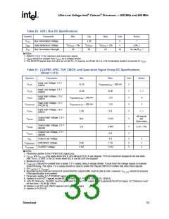
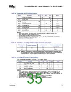
Table 21. CLKREF, APIC, TAP, CMOS, and Open-drain Signal Group DC Specifications
(Sheet 2 of 2)
Symbol
Parameter
Min
Max
Unit
Notes
Input Low Voltage,
VTTPWRGD
VILVTTPWR
0.4
V
7
Input High Voltage,
VTTPWRGD
VIHVTTPWR
1.0
10
V
7
RON
IOL
30
W
3
6
Output Low Current
mA
Leakage Current for Inputs,
Outputs and I/Os
IL
± 100
µA
5
NOTES:
1. Parameter applies to the PWRGOOD signal only.
2. VIlx,min and VIhx,max only apply when BCLK, BCLK# and PICCLK are stopped. PICCLK should be stopped in the low state.
See Tables 28 and 29 for DC levels when BCLK and BCLK# are stopped.
3. Measured at 9 mA.
4. VCMOSREF should be created from a stable 1.5-V supply using a voltage divider. It must track the voltage supply to maintain
noise immunity. The same 1.5-V supply should be used to power the chipset CMOS I/O buffers that drive these signals.
5. (0 ≤ VIN/OUT ≤ VIhx,max).
6. Specified as the minimum amount of current that the output buffer must be able to sink. However, VOL,max cannot be ensured
if this specification is exceeded.
7. Parameter applies to VTTPWRGD signal only.
8. Applies to non-AGTL signals except BCLK, PWRGOOD, PICCLK, BSEL[1:0], VID[4:0].
9. ±5% DC tolerance. CLKREF must be generated from the 2.5-V supply used to generate the BCLK signal. AC Tolerance must
be less than –40 dB @ 1 MHz.
10.Applies to all TAP and CMOS signals (not to APIC signals).
11.Applies to PICD[1:0].
3.6
AC Specifications
3.6.1
System Bus, Clock, APIC, TAP, CMOS, and Open-drain AC
Specifications
All system bus AC specifications for the AGTL signal group are relative to the crossing point of the
rising edge of the BCLK input and falling edge of the BCLK# input. All AGTL timings are
referenced to VREF for both 0 and 1 logic levels unless otherwise specified. All APIC, TAP,
CMOS, and Open-drain signals except PWRGOOD are referenced to 1.0 V. All minimum and
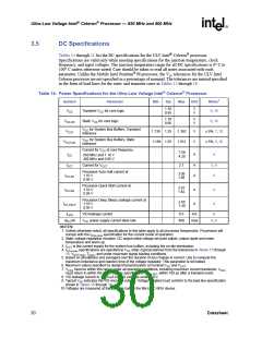
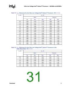
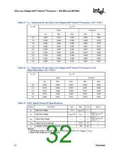
maximum specifications are at points within the power supply ranges shown in Tables 15 through 18
and junction temperatures (Tj) in the range 0° C to 100° C unless otherwise noted. Tj must be less
than or equal to 100° C (or the otherwise-noted given value) for all functional processor states.
34
Datasheet

 INTEL [ INTEL ]