Ultra-Low Voltage Intel® Celeron® Processor — 650 MHz and 400 MHz
‘
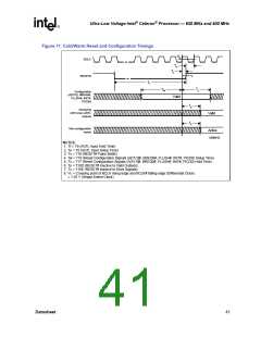
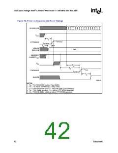
Figure 11. Cold/Warm Reset and Configuration Timings
VC
BCLK
T
u
T
t
RESET#
V
T
v
T
T
x
w
Configuration
(A[15:5], BREQ0#,
FLUSH#, INIT#,
PICD0)
Valid
T
y
PICD[1:0]
AGTL/non-AGTL
outputs
Valid
T
z
Non-configuration
inputs
Active
D0006-02
NOTES:
1. Tt = T9 (AGTL Input Hold Time)
2. Tu = T8 (AGTL Input Setup Time)
3. Tv = T10 (RESET# Pulse Width)
4. Tw = T16 (Reset Configuration Signals (A[15:5]#, BREQ0#, FLUSH#, INIT#, PICD0) Setup Time)
5. Tx = T17 (Reset Configuration Signals (A[15:5]#, BREQ0#, FLUSH#, INIT#, PICD0) Hold Time)
6. Ty = T18D (RESET# inactive to Valid Outputs)
7. Tz = T18E (RESET# inactive to Drive Signals)
8. Vc = Crossing point of BCLK rising edge and BCLK# falling edge (Differential Clock)
= 1.25 V (Single Ended Clock)
Datasheet
41

 INTEL [ INTEL ]