Ultra-Low Voltage Intel® Celeron® Processor — 650 MHz and 400 MHz
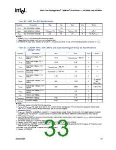
Table 26. Reset Configuration AC Specifications and Power On/Power Down Timings
(Sheet 2 of 2)
Symbol
Parameter
Min
Typ
Max
Unit
Figure
Notes
Time from VCCT-12% to
VTTPWRGD low
T20A
0
ns
12
All outputs valid after VTTPWRGD
low
T20B
T20C
T20D
0
0
0
ns
ns
ns
12
12
12
All inputs required valid after
VTTPWRGD low
VID, BSEL signals valid after
VTTPWRGD low
Measurement
from 300 mV to
900 mV. Amount
of noise (glitch)
less than 100
T20E
VTTPWRGD Transition Time
100
µs
mV. See Section
4.3.1 for details
†
At least 1 ms must pass after PWRGOOD rises above V
specification until RESET# may be deasserted.
and BCLK, BCLK# meet their AC timing
IH18min
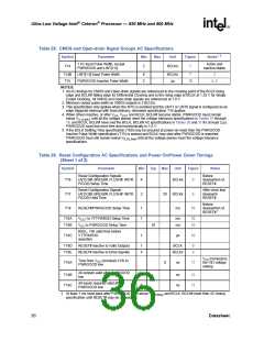
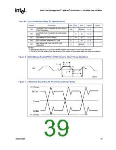
Table 27. APIC Bus Signal AC Specifications
Symbol
Parameter
Min
Max
Unit
Figure
Notes1
T21
T22
T23
T24
T25
T26
T27
T28
PICCLK Frequency
PICCLK Period
2
33.3
500
MHz
ns
2
30
PICCLK High Time
PICCLK Low Time
PICCLK Rise Time
PICCLK Fall Time
PICD[1:0] Setup Time
PICD[1:0] Hold Time
10.5
10.5
0.25
0.25
8.0
ns
at>1.6 V
at<0.4 V
(0.4 V – 1.6 V)
(1.6 V – 0.4 V)
3
ns
3.0
3.0
ns
ns
ns
7
7
2.5
ns
3
PICD[1:0] Valid Delay
(Rising Edge)
1.5
1.5
8.7
T29
ns
6
3, 4
PICD[1:0] Valid Delay
(Falling Edge)
12.0
NOTES:
1. All AC timings for APIC signals are referenced to the PICCLK rising edge at 1.0 V. All CMOS signals are
referenced at 1.0 V.
2. The minimum frequency is 2 MHz when PICD0 is at 1.5 V at reset Referenced to PICCLK Rising Edge.
3. For Open-drain signals, Valid Delay is synonymous with Float Delay.
4. Valid delay timings for these signals are specified into 150 Ω to 1.5 V and 0 pF of external load. For real
system timings these specifications must be derated for external capacitance at 105 ps/pF.
Datasheet
37

 INTEL [ INTEL ]