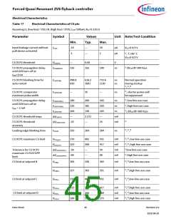
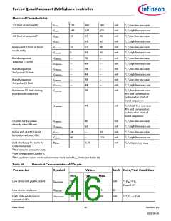
Forced Quasi Resonant ZVS flyback controller
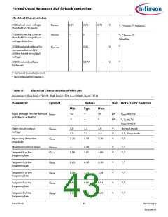
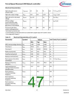
Electrical Characteristics
1), 2) tGD0offZC≥tGD0offZCMin
ZCD output over-voltage
threshold in HV mode
2.72
2.75
2
2.79
V
VZCDOVP
1), 2) tGD0offZC
≥
ZCD debouncing counter
threshold for output over-
voltage detection
—
—
NZCDOVP
tGD0offZCMin
1)
ZCD threshold voltage for
compensation of ZVS
ontime based on output
voltage
2.34
V
V
Vzcd_vout
1)
ZCD threshold voltage
hysteresis
-
0.177
-
1)
Not tested in production test.
2) See configuration Chapter 5.
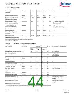
Table 15
Electrical Characteristics of MFIO pin
Assuming LL (low line) =72V, HL (high line) =372V, LPRI=200uH, RCS=0.135 Ω
Parameter
Symbol
Values
Unit Note/Test Condition
Min.
-10
Typ.
—
Max.
10
Input leakage current without
pull device activated
µA
µA
IMFIOLK
V
MFIO=0 V/3 V
1), TJ=85˚C
V
-1
—
1
MFIO=0 V/3 V
Open circuit output
voltage
3.0
3.3
3.6
V
V
V
Normal mode
VMFIOOC
3.0
3.2
3.4
1), 2), sleep mode
1) 3)
Open-loop detection
threshold
2.25
2.30
2.36
,
VMFIOH
1) 3)
Maximum control range
—
2.30
1.61
—
V
V
,
VMFIOmax
VMFIOB
1) 3)
Setpoint B of the
frequency law
1.56
1.66
,
1) 3)
Setpoint C of the
frequency law
2.25
1.19
0.82
0.17
2.30
1.23
0.86
0.21
2.36
1.28
0.91
0.25
V
V
V
V
,
VMFIOC
VMFIOD
VMFIOD
VMFIOD
1) 3)
Setpoint D of the
frequency law
,
1) 3)
Setpoint E of the
frequency law
,
1) 3)
Setpoint F of the
frequency law
,
Data Sheet
43
Revision 2.0
2020-08-20

 INFINEON [ Infineon ]