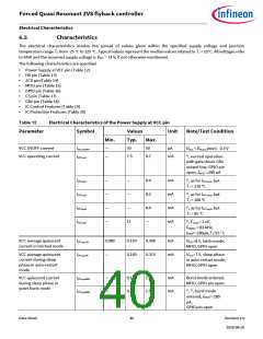
Forced Quasi Resonant ZVS flyback controller
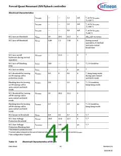
Electrical Characteristics
6.5
Characteristics
The electrical characteristics involve the spread of values given within the specified supply voltage and junction
temperature range TJ from -25 °C to 125 °C. Typical values represent the median values related to TJ = 25°C. All voltages refer
to GND and the assumed supply voltage is VVCC = 14 V, if not otherwise mentioned.
The following characteristics are specified
•
•
•
•
•
•
•
•
•
Power Supply at VCC pin (Table 12)
HV pin (Table 13)
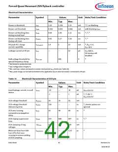
ZCD pin(Table 14)
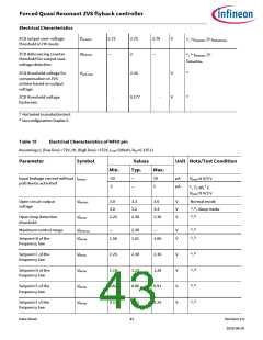
MFIO pin (Table 15)
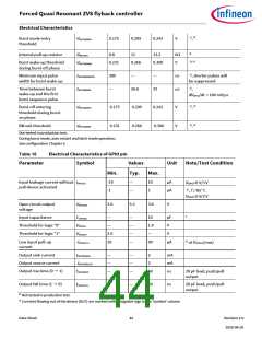
GPIO pin (Table 16)
CS pin (Table 17)
GDx pin (Table 18)
IC Control Features (Table 19)
IC Protection Features (Table 20)
Table 12
Electrical Characteristics of the Power Supply at VCC pin
Parameter
Symbol
Values
Unit
Note/Test Condition
Min.
—
Typ.
30
Max.
50
VCC UVOFF current
µA
IVCCUVOFF
IVCCop1
VVCC < VVCCon(min) - 0.3 V
1), normal operation
with gate driver GDx
output low, GPIO pin
open, IMFIO-=280 µA
VCC operating current
—
7.5
8.7
mA
—
—
—
—
—
—
—
11
8.4
8.2
8.0
—
mA
mA
mA
mA
IVCCop2
IVCCop3
IVCCop4
IVCCop5
1), as for IVCCop1, but
TJ = 110 °C
1), as for IVCCop1, but
TJ = 100 °C
1), as for IVCCop1, but
TJ = 85 °C
1), Cload = 2 nF,
f
SWGDx = 83 kHz,
IMFIO=-280µA,TJ=25˚C
VCC average quiescent
current in latched mode
0.080
0.150
0.160
0.300
0.310
mA
mA
IVCCquLM
IVCCquAR
V
VCC=8 V, latch mode,
MFIO, GPIO open
VCC average quiescent
current during sleep
phase in auto-restart
mode
—
V
VCC=7 V, sleep phase
in auto-restart mode,
MFIO, GPIO open
VCC quiescent current
during sleep phase in
quiet burst mode
—
—
0.18
0.46
1.2
1.5
mA
mA
Burst mode entered,
MFIO, GPIO pin open
IVCCquBM1
IVCCquBM2
1), 2), burst mode
entered, IMFIO=-280
µA,
GPIO pin open
Data Sheet
40
Revision 2.0
2020-08-20

 INFINEON [ Infineon ]