Forced Quasi Resonant ZVS flyback controller
Electrical Characteristics
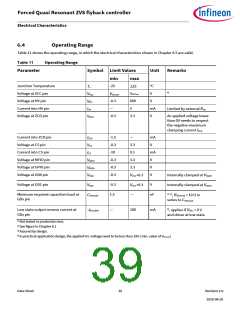
6.4
Operating Range
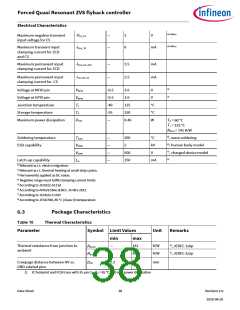
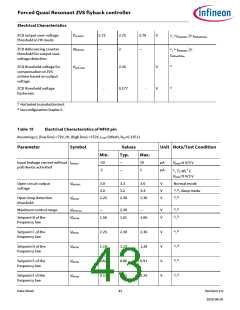
Table 11 shows the operating range, in which the electrical characteristics shown in Chapter 6.5 are valid.
Table 11
Operating Range
Parameter
Symbol Limit Values
Unit
Remarks
min
max
Junction Temperature
Voltage at VCC pin
Voltage at HV pin
-25
°C
V
TJ
125
VVCCon
600
5
4)
VVCC
VHV
IHV
VVCCoff
-0.3
—
V
Current into HV pin
Voltage at ZCD pin
mA
V
Limited by external RHV
-0.3
3.3
An applied voltage lower
than 0V needs to respect
the negative maximum
clamping current IZCD
VZCD
Current into ZCD pin
Voltage at CS pin
-1.5
-0.3
-10
—
mA
V
IZCD
3.3
0.1
3.3
3.3
VCS
Current into CS pin
Voltage at MFIO pin
Voltage at GPIO pin
Voltage at GD0 pin
mA
V
ICS
-0.3
-0.3
-0.3
VMFIO
VGPIO
VGD0
V
V
V
V
VCC+0.3
VCC+0.3
Internally clamped at VGD0H
Internally clamped at VGD1H
Voltage at GD1 pin
-0.3
1.5
V
VGD1
1), 2), RGDxload = 10 Ω in
series to CGDxload
Minimum required capacitive load at
GDx pin
—
nF
CGDxload
Low state output reverse current at
GDx pin
—
100
mA
-IGDxLREV
3), applies if VGDx < 0 V
and driver at low state
1) Not tested in production test.
2) See figure in Chapter 8.1
3) Assured by design.
4) In practical application design, the applied Vcc voltage need to be less than 19V ( min. value of VVCCon
)
Data Sheet
39
Revision 2.0
2020-08-20

 INFINEON [ Infineon ]