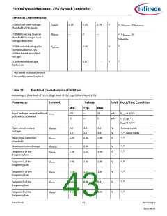
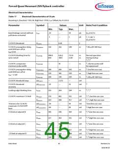
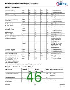
Forced Quasi Resonant ZVS flyback controller
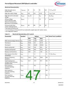
Electrical Characteristics
High state peak source
current of GD0
30
35
41
mA
-IGD0HPKSRC
2), 3), CLoad=2 nF
3), IGDx=-1 mA
High state output voltage
9.97
10.5
11.03
V
V
VGDxH
High state rail-to-rail output
voltage
—
VGDxHRR
V
VCC-0.5
VVCC
V
VCC<VGDxH
APD low voltage
—
—
1.6
V
VGDxAPD
IGDx=5 mA
(active pull down while
device is not powered or
gate driver is not enabled)
Permanent pull-down
resistor inside gate driver
450
600
750
kΩ
RGDxPPD
1)
Not tested in production test.
2)
Currents flowing out of the device (DUT) are marked with a negative sign in the ‘Symbol’ column.
3)
See configuration Chapter 5.
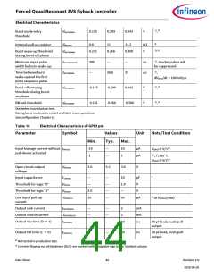
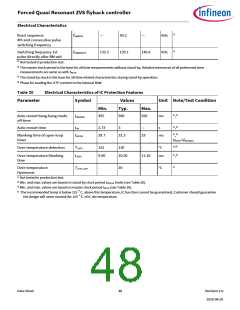
Table 19
Electrical Characteristics of IC Control
Parameter
Symbol
Min.
Values
Typ.
Unit Note/Test Condition
Max.
2.459
54.78
109.56
VREF internal voltage reference
Time base 1
2.397
49.50
99.0
15.0
9.09
6.64
—
2.428
52.1
104.28
15.8
10.0
7.0
V
VREF
1)
µs
tBase1
tBase2
tMCLK
tSTBCLK
tSSmax
tBootIC
1)
Time base 2
µs
2)
Master clock period
Stand-by clock period
Maximum soft-start time
16.6
11.11
7.36
—
ns
3)
µs
1)
ms
1),4), VVCC>VVCCon
Boot sequence time when
activating IC
1.2
ms
1)
Maximum frequency
operation
132.3
21.9
139.1
23.0
146.6
24.3
kHz
fSWmax
fSWmin
1)
Switching frequency
setting at minimum power
operation point
kHz
1)
Burst sequence:
1st pulse switching
frequency
—
—
—
50.2
50.2
50.2
—
—
—
kHz
fSWBSP1
fSWBSP2
fSWBSP3
1)
Burst sequence:
2nd pulse switching
frequency
kHz
1)
Burst sequence:
3rd pulse switching
frequency
kHz
Data Sheet
47
Revision 2.0
2020-08-20

 INFINEON [ Infineon ]