Forced Quasi Resonant ZVS flyback controller
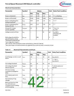
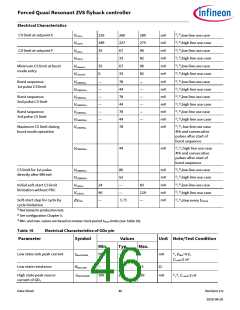
Electrical Characteristics
Parameter
Symbol
Values
Unit Note/Test Condition
Min.
1.10
Typ.
1.156
0.443
Max.
1.21
1),2), no blanking
with blanking tHVBO
1), 2), 3)
Brown-in threshold
Brown-out threshold
mA
mA
ms
IHVBI
0.420
0.465
IHVBO
tHVBO
Brown-out blanking time
during normal load
0.99
4.95
2.4
1.09
5.27
5
1.21
5.59
10
1) 2)
Brown-out blanking time
during soft-start
ms
mA
,
tHVBOSS
IHVchargeVCC
IHVLK
4), VVCC=1 V,
VHV=30 V
HV peak VCC charge
current capability
Leakage current at HV pin
—
—
10
µA
V
VHV=600 V,
HV startup cell
disabled
1)
Bulk voltage threshold for
special frequency clamp
1) Not tested in production test.
Vbulk_high
200
2) See configuration Chapter 5.
3) Min. and max. values are based on master clock period tMCLK limits (see Table 20).
4) Max. peak charge current will be limited in the application by an external resistor connected to HV pin.
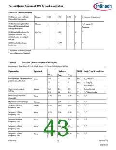
Table 14
Electrical Characteristics of ZCD pin
Parameter
Symbol
Min.
Values
Unit Note/Test Condition
Typ.
Max.
Input leakage current, no pull
device
-10
—
10
µA
µA
IZCDLK
V
ZCD=0 V/3 V
1), TJ=85˚C
-1
—
1
V
ZCD=0 V/3 V
ZCD voltage threshold
20
35
55
mV
ns
VZCDTHR
tZCDPW
ZCD voltage threshold
debouncing time
150
—
—
1), shorter pulses are
ignored
1)
ZCD zero crossing
comparator propagation
delay
20
40
60
ns
tZCDP
1) 2)
ZCD ringing suppression
time
570
150
—
608
180
—
647
220
3.33
ns
,
tZCDRS
ZCD clamping of neg.
voltages
mV
µs
-VZCDclp
tGD0offZCMin
1)
Minimum time from GD0
turn off to first zero-
crossing to ensure settling
of ZCD sampling
Data Sheet
42
Revision 2.0
2020-08-20

 INFINEON [ Infineon ]