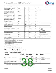
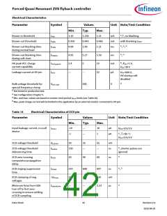
Forced Quasi Resonant ZVS flyback controller
Electrical Characteristics
4)<500ns
4)<500ns
Maximum negative transient
input voltage for CS
—
—
3
6
V
-VCS_TR
-ICLN_TR
Maximum transient input
clamping current for ZCD
and CS
mA
Maximum permanent input
clamping current for ZCD
—
—
3.5
2.5
mA
mA
-ICLN_DC_ZCD
Maximum permanent input
clamping current for CS
-Icln_DC_CS
3)
3)
Voltage at MFIO pin
-0.5
-0.5
-40
-55
—
3.6
V
VMFIO
VGPIO
TJ
Voltage at GPIO pin
3.6
V
Junction temperature
Storage temperature
Maximum power dissipation
125
150
0.46
°C
°C
W
TS
PTOT
TA = 60 °C
TJ = 125 °C
RthJA = 141 K/W
Soldering temperature
ESD capability
—
—
—
—
260
2
°C
kV
V
5), wave soldering
TSold
VHBM
VCDM
ILU
6), human body model
500
150
7), charged device model
8)
Latch-up capability
1) Relevant w.r.t. electro migration.
mA
2) Relevant w.r.t. thermal heating at small duty cycles.
3) Permanently applied as DC value.
4) Negative range must fulfill clamping current limits
5) According to JESD22-A111A
6) According to ANSI/ESDA/JEDEC JS-001-2012
7) According to JESD22-C101F
8) According to JESD78D, 85 °C (Class II) temperature
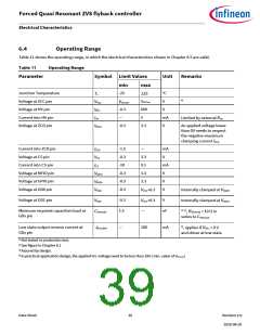
6.3
Package Characteristics
Table 10
Thermal Characteristics
Symbol Limit Values
Parameter
Unit
Remarks
min
—
max
1), JEDEC 1s0p
1), JEDEC 2s2p
Thermal resistance from junction to
ambient
141
K/W
K/W
RthJA1
RthJA2
—
81
Creepage distance between HV vs.
GND-related pins
3.3
—
mm
DCR
1) IC footprint and PCB trace with 35 µm Cu, TA = 85 °C, 180 mW power dissipation
Data Sheet
38
Revision 2.0
2020-08-20

 INFINEON [ Infineon ]