Forced Quasi Resonant ZVS flyback controller
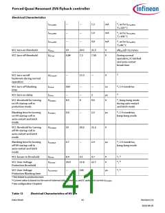
Electrical Characteristics
6
Electrical Characteristics
All signals are measured with respect to ground GND pin. The voltage levels are valid if other ratings are not violated.
Attention: Limits are subject to change according to test engineering results
6.1
Definitions
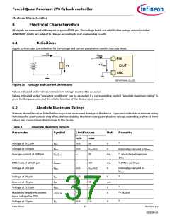
Figure 30 illustrates the definition for the voltage and current parameters used in this data sheet.
+I
+IPIN
PIN
+
+VPIN
DUT
+V
_
GND
DEFINITIONS_V_I_DS
Figure 30 Voltage and Current Definitions
Values indicated under “absolute maximum ratings” must not be exceeded.
Values indicated under “operating conditions” can be exceeded if a corresponding explicit “absolute maximum rating” is
given for this parameter, but the related function of the device is not ensured.
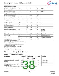
6.2
Absolute Maximum Ratings
Stresses above the values listed below may cause permanent damage to the device. Exposure to absolute maximum rating
conditions for given periods may affect device reliability. Maximum ratings are absolute ratings; exceeding anyone of these
values may cause irreversible damage to the device.
Table 9
Absolute Maximum Ratings
Symbol
Parameter
Limit Values
Unit Remarks
min
-0.5
-0.5
—
max
3)
Voltage at VCC pin
26
V
VVCC
VGD0
Voltage at GD0 pin
V
V
VCC+0.3
Internally clamped to VGD0H
1), absolute average over
1 ms
Average current at GD0 pin
20
mA
|IGD0 AVG
|
RMS Current at GD0 pin
Voltage at GD1 pin
—
100
mA
V
2), RMS over 20 µs
IGD0RMS
VGD1
-0.5
Internally clamped to
VGD1H
V
VCC+0.3
3)
Voltage at HV pin
Current at HV pin
Voltage at ZCD pin
-0.5
—
600
10
V
VHV
mA
V
IHV
3)
-0.5
—
3.6
2.0
VZCD
-VZCD_TR
Maximum negative transient
input voltage for ZCD
V
4) <500ns
3)
Voltage at CS pin
Data Sheet
-0.5
3.6
V
VCS
37
Revision 2.0
2020-08-20

 INFINEON [ Infineon ]