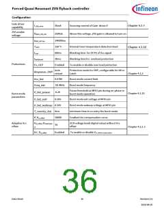
Forced Quasi Resonant ZVS flyback controller
Configuration
Gate driver
capability
35mA
Sourcing current of Gate driver 0
I_GD0_drive
Chapter 4.2.7
Chapter 4.3.10
ZVS enable
voltage
250Vdc
Above this voltage ,ZVS gate is allowed to turn on
VBULK_ZVS_ON
140000ns
130 °C
tMAX_OnTime
TJOTP
Internal Over-temperature detection level
Blanking time for OCP2 of Vcs signal
Blanking time for overload protection
To enable or disable over load protection
600ns
tocp2
30ms
tpeakpower
En_OLP
Protections
Enabled
Auto
restart
Protection mode for OVP, configurable for AR or
Latch
Response_OVP
Chapter 4.1.5
Chapter 4.2.10
0.078V
Burst mode current limit
Burst mode frequency
Vcs_bst
50.4kHz
Freq_bst
Pause threshold at MFIO pin during on-phase in
burst mode operation
0.2V
V_bst_pause
Burst mode
parameters
0.26V
0.26V
0ms
Burst mode exit voltage at MFIO pin
Burst mode wakeup voltage at MFIO pin
minimum time to re-entry the burst mode
Gradient for compensation curve
V_bst_exit
V_bst_wakeup
T_reentry_bst
K_Vcs_offset
20000
Vcs_offset_Vzcdzeropoi
nt
Adaptive Vcs
offset
ZCD voltage level( digital value) without Vcs
offset
79
Chapter 4.2.1.3
Enabled
To enable or disable Vcs_offset compensation
En_Vcs_offset
Data Sheet
36
Revision 2.0
2020-08-20

 INFINEON [ Infineon ]