Forced Quasi Resonant ZVS flyback controller
Functional Description
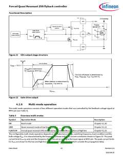
ZVS-winding
VCC
VCC
Power
MOSFET
VD
Source current
control
IGD1HPKSRC
Q2
CGD
Gate driver
state control
RGD1
FFR mode
pulse control
GD1
CGS
VGD1H
RGD1LSNK
GND
Figure 21 GD1 output stage structure
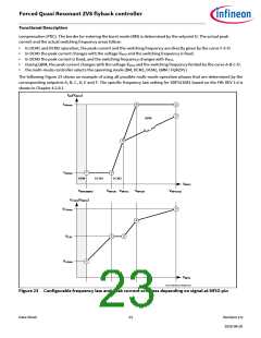
VGDx(t)
turn-on phase
VGDxH = 10.5 V
dVGDx/dt is determined
by IGDxHPKSRC and CGS
The turn-off phase is determined by
RGDx, RGDxLSNK, CGS, CGD and VD
Miller plateau is determined by
IGDxHPKSRC, CGD and VD
t
tGDxon
Figure 22 Gate drive output
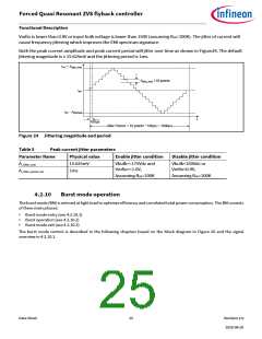
4.2.8
Multi-mode operation
The multi-mode operation consists of two different operation modes that are controlled by the feedback voltage signal at
MFIO pin (see Table 3).
Table 3
Overview multi-modes
Symbol
BM
Operation Mode
Description
Burst mode
Chapter 4.2.10
Chapter 4.2.11
Chapter 4.2.12
QRM
Quasi resonant mode at low line
FQRZVSM
Forced quasi resonant ZVS mode during BM and DCMx operation at high line
The configurable multi-mode operation depends on the inductance design, switching frequency, load condition and the
bulk voltage VBulk. It is characterized by the frequency scheme and peak current correlation shown in Figure 23. The peak
current limit VCSPK (y-axis) and the frequency limits are set according to the input signal at MFIO pin. The peak current limits
for VCSPK are shown for the low and high-line use case (see Chapter 4.2.3), which consider the propagation delay
Data Sheet
22
Revision 2.0
2020-08-20

 INFINEON [ Infineon ]