Forced Quasi Resonant ZVS flyback controller
Functional Description
4.2.4
Soft-start
The IC control provides a soft-start during initial startup and auto-restart cycles. The soft-start slew rate is defined by the
step ∆VCSS = 1.7 mV taking place every time step of tBase1 = 52.14 µs. Furthermore, the peak current start level is determined
by the parameter VCSSS
.
The soft-start phase is latest finished after VCS has ramped up to the maximum level of VCSmax (see Figure 18).
The total soft-start time tSSmax is therefore based on the following equation:
푽
ꢀ푽
푪푺풎풂풙
푪푺푺푺
풕푺푺풎풂풙 = 풕푩풂풔풆ퟏ
∙
( 9 )
∆푽
푪푺푺
The associated ramped up peak current limitation is determined by internal digital numbers, which are not depending on
the propagation delay during peak current limitation process.
VCS(t)
tSSmax
VCSmax
tBase1
DVCSS
VCSSS
t
Figure 18 Soft-start timing
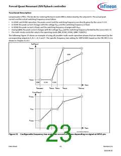
The internal soft-start phase is finished once the voltage level at MFIO pin is getting lower than 2.42 V. Then the setting for
CS limitation is determined by the feedback signal at MFIO pin via the frequency law (see Chapter 4.2.8.1).
4.2.5
Leading edge blanking (LEB) at CS pin
A digital leading edge blanking filter with tCSLEB = 269 ns (see Chapter 5) is integrated in the OCP1 peak current control path
to prevent the current limitation process from distortions, caused by the leading edge spike at the switch-on of the power
MOSFET (see Figure 19). The LEB applies only for the OCP1 comparator (see Figure 3) that is used for cycle-by-cycle peak
current limitation. The LEB needs also to ensure a monotonous peak current control without being impacted by ringing
taking place directly after the leading edge spike.
VGD0(t)
t
VCS(t)
tCSLEB
VCSOCP1
t
Figure 19 Leading edge blanking
Data Sheet
20
Revision 2.0
2020-08-20

 INFINEON [ Infineon ]