Forced Quasi Resonant ZVS flyback controller
Functional Description
VVDDP = 3.3 V
RMFIOPU
MFIO
C3
BM Exit
VMFIOBMEX1
C5
Power
Management
VMFIOBMWK
burst-on
BM 2-point
Regulation
BM Ctrl
burst-off
C6
C7
VMFIOBMPA
Frequency
Law
BM Entry
VMFIOBMEN
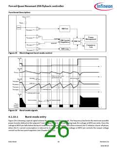
Figure 25 Block diagram burst mode control
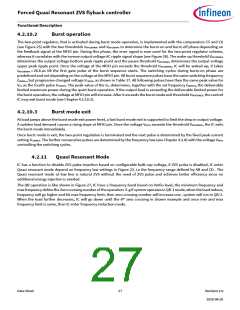
IOUT(t)
t
t
VOUT(t)
VOUTnom
Wake-up when wake-
up threshold met
tMFIOBMWK
exit burst mode
VMFIO(t)
VMFIOBMEX
wake-up
VMFIOBMWK
VMFIOBMPA
entering pause
VMFIOBMEN
t
entering burst mode
burst-on phase
VCS(t)
burst-off (pause) phase
VCSmin,
VCSBSP4,
VCSBMEX
t
Figure 26 Burst mode signals
4.2.10.1
Burst mode entry
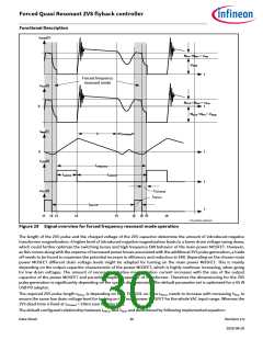
Figure 26 is showing a typical signal scheme for entering quiet burst mode. The frequency law limits the minimum possible
power transfer defined at the setpoint F (see Chapter 4.2.8.1). With decreasing load, the voltage at MFIO pin sinks. Once the
voltage at MFIO pin falls below the burst mode entry threshold VMFIOBMEN, BM is then entered, the IC initiates a burst-off phase,
where the IC current consumption is reduced to IVCCquBM2. Afterwards, the voltage at MFIO pin controls the output voltage
control via the two-point regulator (see Chapter 4.2.10.2).
Data Sheet
26
Revision 2.0
2020-08-20

 INFINEON [ Infineon ]