Forced Quasi Resonant ZVS flyback controller
Functional Description
4.2.6
Spike blanking at CS pin for 2nd level over-current detection
(OCP2)
A further comparator OCP2 is implemented at CS pin (see Figure 3) to detect dangerous current levels (see Chapter 5), which
could occur if one or more transformer windings are shorted or if the secondary side diode is shorted. To avoid an accidental
trigger by exceeding this 2nd level over-current protection threshold VCSOCP2 = 0.6 V, a spike blanking time tCSOCP2BL = 616.2 ns
(see Chapter 5) is implemented in the output path of the OCP2 comparator.
4.2.7
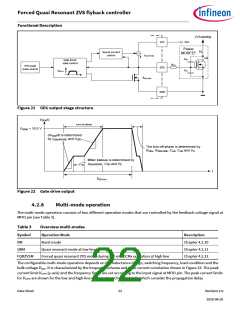
Gate driver output GD0 and GD1
The gate driver GD0 and GD1 are of the same type. The GD0 is used for controlling the main MOSFET connected to the primary
main inductance of the flyback transformer. The GD1 is used for controlling the FQR ZVS mode (see Chapter 4.2.8) by driving
the dedicated MOSFET that is connected to the ZVS winding at the flyback transformer.
The gate driver output stages consist of a regulated current source connected to VCC pin and a MOSFET switch connected
to GND (see Figure 20 and Figure 21). The peak source current at GDx is set to IGDxHPKSRC = -35 mA. The MOSFET switch provides
a discharge path for the main power MOSFET with a sink capability of RGDxLSNK ≤ 6.5 Ω.
The controlled source current determines together with the gate-source capacitance CGS and the gate-drain capacitance CGD
of the external power MOSFET the rising slope during turn-on phase (see Figure 22). The gate driver state control ensures
that the charged gate driver output voltage is clamped at the level VGDxH = 10.5 V.
The external gate resistor RGDx is therefore only meant for adjusting the peak sink current and the corresponding gate voltage
falling slope during the turn-off phase. Here the turn-on behavior is mainly dominated by the controlled limited current
source IGDxHPKSRC as the size of the external gate resistor is mainly limiting the higher peak sink current at GDx pin. When
dimensioning the serial gate resistor RGDx, also a minimum load capacitance needs to be considered after RGDx (see Chapter
9.1), which needs to be provided by the corresponding gate-source capacitance CGS of the external power MOSFET. This
ensures a smooth and stable settling of the voltage level VGDxH at the end of the turn-on phase.
Primary main
inductance
VCC
VCC
Power
MOSFET
VD
Source current
control
IGD0HPKSRC
Q1
CGD
CGS
CS
Gate driver
state control
RGD0
Flyback
ctrl
GD0
GND
VGD0H
RGD0LSNK
RCS
Figure 20 GD0 output stage structure
Data Sheet
21
Revision 2.0
2020-08-20

 INFINEON [ Infineon ]