Forced Quasi Resonant ZVS flyback controller
Functional Description
So for Vzcd=1.69V, Vo will be 1.69*2/2*(39+5.6)/5.6=13.46V assuming transformer coupling is 1.
For Vzcd=1.2V, Vo will be 1.2*2/2*(39+5.6)/5.6=9.56V.
This means that when output voltage is above 13.46V, there is no Vcs offset compensation, below 9.56V the compensation is
clamped at 38mV as calculated above.
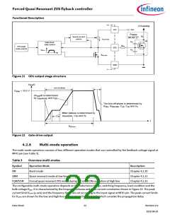
Vzcd
Vzcd_zero_point
Kvcs_offset
Vzcd_LowV
Vcs offset
Vcs_offset
VCSOFFSET
Figure 16 Vcs_offset calculation
4.2.2
Vbulk voltage measurement via HV startup cell
The VBulk voltage is measured via the HV pin that is connected at the bulk capacitor node. The current IHV is sampled in the IC
and processed for the following functions:
•
•
•
Brown-in protection ( Chapter 4.3.4)
Brown-out protection (Chapter 4.3.5),
Propagation delay compensation (Chapter 4.2.3),
In all these functions, the current IHV represents the bulk voltage.
4.2.3
Propagation delay compensation (PDC)
Due to the gate driver turn-off propagation delay tPD, the level VCSOCP1 set by the OCP1 comparator will not directly control
the inductor peak current, ILPk
.
Without propagation delay, the peak current would be given by ILPk = RCS-1·VCSOCP1. However, due to the propagation delay,
the OCP1 level is exceeded by
푹푪푺 ∙ 푰푳풑풌 = 푽푪푺푶푪푷ퟏ + 푽푪푺푷푫(푽푩풖풍풌
)
( 5 )
Where the propagation delay overshoot VCSPD(VBulk) is
푹
푪푺
푽푪푺푷푫(푽푩풖풍풌) =
∙ 풕푷푫 ∙ 푽푩풖풍풌
( 6 )
푳
푷풓풊
In Figure 17 related example waveforms are presented.
Data Sheet
18
Revision 2.0
2020-08-20

 INFINEON [ Infineon ]