Forced Quasi Resonant ZVS flyback controller
Functional Description
vGD0(t)
vGD0(t)
t
t
t
t
vDrain(t)
vDrain(t)
VBulkHL
VBulkLL
vCS(t)
vCS(t)
tPD
tPD
tCS
RCSILpk
(t)
RCSILpk(t)
tCS
dvCS/dt
dvCS/dt
t
t
MULTIMODE_PDC
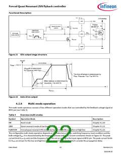
Figure 17 Propagation Delay and Propagation Delay Compensation
On the left side, the bulk voltage is low, the slope of inductor current and of the CS voltage are low, too. When the CS voltage
reaches the OCP1 level, the gate driver turns off and the inductor current reaches its peak after the turn off propagation
delay tPD. The turn off propagation delay tPD includes the delay tCS of the filter capacitor connected to CS pin and the resistor
connected between shunt resistor and CS pin (see Typical Application Figure). The overshoot of the inductor current due to
propagation delay is small due to the small slope
풅푽
푹
∙푽
푪푺
푪푺 푩풖풍풌
=
( 7 )
풅풕
푳
풑
The right side of Figure 17 shows the same operating waveforms for a higher bulk voltage. In this case, the OCP1 comparator
limit needs to be less than on the left side to reach the same inductor peak current. Although the propagation delay remains
the same, the slope as well as the overshoot due to propagation delay is larger.
The XDPS21081 controller is defined to measure the HV current IHV representing the bulk voltage VBulk. The OCP1 comparator
limit is adjusted depending on the measured bulk voltage so that the real peak current due to the propagation delay is
compensated. For this HV pin needs to be connected to VBulk
.
Consequently, any CS peak parameter VCSx is specified in the electrical characteristics (Chapter 6.5) for a low-line use case
(VCSxLL) and for a high-line use case (VCSxHL).
Low-Line Use Case (LL)
•
•
IHVLL = 70 µA as for VBulk = 72 V, RHV = 100 kΩ
(dvCS /dt)LL = 49 mV/µs as for VBulk = 72 V, LPri = 200 µH, RCS = 0.135 Ω
High-Line Use Case (HL)
•
•
IHVHL = 370 µA as for VBulk = 372 V, RHV = 100 kΩ
(dvCS /dt)HL = 251 mV/µs as for VBulk = 372 V, LPri = 200 µH, RCS = 0.135 Ω
These use cases set the corners of the propagation delay compensation which operates in a linear manner so that the typical
OCP1 threshold for any IHV is given by
(
)
ꢀ푽
푽
푰
푽
ꢀ푽
푪푺풙 푯푽
푪푺풙푳푳
푪푺풙푯푳 푪푺풙푳푳
=
( 8 )
푰
ꢀ푰
푰
ꢀ푰
푯푽 푯푽푳푳
푯푽푯푳 푯푽푳푳
Data Sheet
19
Revision 2.0
2020-08-20

 INFINEON [ Infineon ]