Forced Quasi Resonant ZVS flyback controller
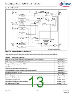
Functional Description
tGD0offZC
vGD0(t)
tf
tOsc/4
tZCDRS
t
vZCD(t)
Voltage sampling
DVZCDOFFSET
VZCDSEC(VSec
)
VZCDVO(VOut
)
VZCDTHR
t
VZCDclp
Ringing
suppression
VOLTAGE_SENSING_SIGNALS_ZCDSH
Figure 15 Output Voltage Sensing Signals
4.2.1.2
Ringing suppression time
To prevent erroneous ZCD events due to primary side gate driver turn off ringing, a ringing suppression time tZCDRS = 0.6µs
applies for the zero-crossing events. During this time no zero-crossing is considered.
4.2.1.3
Vcs offset calculation based on output voltage sensed at ZCD pin
To limit the output current at different output voltage, a linear scaled Vcs offset is inserted to the peak current command.
This offset will be minused from the current command mapping from the frequency law curve.
It is an inverse of the output voltage based on positive ZCD winding voltage. Figure 16 shows when the Vzcd is at
Vzcd_zero_point, the Vcs offset is zero. While Vzcd voltage is at minimum level, the Vcs offset is maximum. The Vcs offset level
depends on the slew rate of Kvcs_offset and the starting point of Vzcd. The equation is as below:
푽풄풔풐풇풇풔풆풕 = 푲풗풄풔풐풇풇풔풆풕 ∗ (푽풛풄풅 − 푽풛풄풅_풛풆풓풐_풑풐풊풏풕)/ퟔퟓퟓퟑퟔ
( 3 )
All the number in above equation is decimal digital value.
At ZCD pin, the sensed voltage will minus 1.2V offset first, then feed into an ADC channel to get the sense the voltage. Also
due to the ADC input voltage range is 1.2-2.8V, so any ZCD voltage out of this range is ignored by the IC and ADC converter
value will be saturated at its min(0) and max value(255).
Below is the example on how to set the value,
Vzcd_zero_point is the voltage level without compensation, here we choose Vzcd=1.69V, the digital value of Vzcd_zero_point_dig=(1.69-
1.2)*1.5/2.4*256=79, Kvcsoffset=20000, for Vzcd=1.2V, the digital value of it will be
Vzcd_dig=(1.2-1.2)*1.5/2.4*256=0, so Vcsoffset_dig=20000*(0-79)/65536=24, its analog value will be 24/256*400=38mV.
If system parameters like transformer turns ratio, ZCD pin voltage divider is known, then the corresponding output voltage
can be calculated. E.g. Naux=2, Nsec=2, RzcdH is 39kohm, RzcdL is 5.6kohm.
푵
풔풆풄
푽풐 = 푽풛풄풅
∗
∗ (푹풛풄풅푳 + 푹풛풄풅푯)/푹풛풄풅푳
( 4 )
푵
풂풖풙
Data Sheet
17
Revision 2.0
2020-08-20

 INFINEON [ Infineon ]