Forced Quasi Resonant ZVS flyback controller
Functional Description
NSec:NAux
RZCDH
iZCD=0
vZCD>0
vSec(t)
vAux(t)
ZCD
GND
RZCDL
ZCD
+
vZCDSEC(vSec
)
GND
VOLTAGE_SENSING_ZCDSH
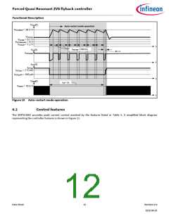
Figure 14 Secondary Side Voltage Sensing
No current clamping applies during the free-wheeling time and the voltage at ZCD pin is given by
푽
푨푼푿
푽풁푪푫푺푬푪(푽푺풆풄) = 푹풁푪푫∙
(
)
( 2 )
푹
풁푪푫푯
RZCD is the internal resistance of VZCDSEC (VSec)and is the equivalent parallel resistance of RZCDH and RZCDL. The related waveforms
are presented in Figure 15. After the primary side gate driver is turned off, the auxiliary voltage goes from its negative level
to positive. After a ringing phase, the positive level is given by the output voltage plus the secondary side diode voltage drop.
During the free-wheeling phase the secondary side diode operates in the linear region until the demagnetization current
becomes very small. This linear relationship can be described as a resistor RDSonSec, resulting in a falling slope according to
RDSonSec·iLSec(t). The secondary side current iLSec(t) decreases with a slope given by the output voltage and the transformer
secondary side inductance. Hence the resulting auxiliary winding voltage is more or less constant until the secondary side
current becomes zero. The reflected voltage at auxiliary winding is sampled at the end of the ringing suppression time (see
Chapter 4.2.1.2). The measured voltage VZCDSEC includes the output voltage level and a superimposed offset ∆VZCDOFFSET that is
depending on the secondary side chosen rectification approach and the associated component dimensioning.
To ensure an accurate measurement of the reflected output voltage, the system dimensioning must provide a free-wheeling
phase that only finishes after the ringing suppression time tZCDRS
.
Furthermore following effects can influence the output voltage sensing if not properly considered in system dimensioning:
•
•
VCC and ZVS capacitor charging
Voltage drop on secondary side at the free-wheeling diode or the secondary side switch
The VCC and ZVS capacitors need to be charged up before the ringing suppression time tZCDRS ends. The superimposed
voltage offset ∆VZCDOFFSET at sample time point due to secondary side rectification approach needs to be considered either by
the dimensioning of the ZCD resistor divider or the internal overvoltage threshold setting VZCDOVP (see Chapter 4.3.11).
Data Sheet
16
Revision 2.0
2020-08-20

 INFINEON [ Infineon ]