OPTIREG™ SBC TLE9274QXV33
Serial Peripheral Interface
14.3
SPI programming
For the TLE9274QXV33, 7 bits are used for the address selection (6...0). Bit 7 is used to decide between
Read_Only and Read_Clear for the status bits, and between Write and Read Only for configuration bits. For the
actual configuration and status information, 8 data bits (BIT15...8) are used.
Writing, clearing and reading is done byte wise. SPI configuration and status bits are not cleared automatically
and must be cleared by the microcontroller, e.g. if the TSD2 was set due to overtemperature. The
configuration bits will be partially automatically cleared by the SBC - please refer to the individual registers
description for detailed information. During SBC Restart mode or Sleep mode or Fail-Safe mode, the SPI
communication is ignored by the SBC, i.e. it is not interpreted.
There are two types of SPI registers:
•
•
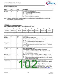
Control registers: The registers used to configure the SBC, e.g. SBC mode, watchdog trigger, etc.
Status registers: The registers used to signal the status of the SBC, e.g. wake-up events, warnings, failures,
etc.
For the status registers, the requested information is given in the same SPI command in DO.
For the control registers, the status of the respective bit is also shown in the same SPI command, but if the
setting is changed this is only shown with the next SPI command (it is only valid after CSN HIGH) of the same
register.
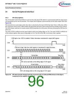
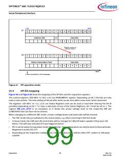
The SBC status information from the SPI status registers is transmitted in a compressed format with each SPI
response on SDO in the so-called Status Information Field register (see also Figure 47). The purpose of this
register is to quickly signal the information to the microcontroller if there was a change in one of the SPI status
registers. In this way, the microcontroller does not need to constantly read all the SPI status registers but only
those registers that have changed. Each bit in the Status Information Field represents an SPI status register
(see Table 22). As soon as one bit is set in one of the status registers, the respective bit in the Status
Information Field register is set. The register WK_LVL_STAT is not included in the status Information field. This
is shown in Table 22.
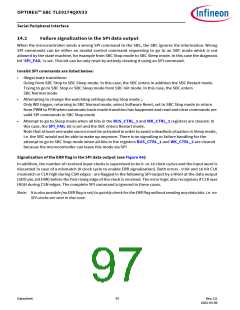
For example, if bit 0 in the Status Information Field is set to 1, one or more bits of the register 100 0001
(SUP_STAT) are set to 1. Then this register needs to be read in a second SPI command. The bit in the Status
Information Field will be set to 0 when all bits in the register 100 0001 are set back to 0.
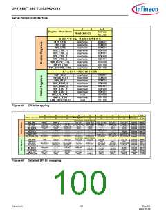
Table 22 Status information field
Status
Symbol
Status register
information bit address bit
0
1
2
3
4
5
6
7
100 0001
100 0010
100 0011
100 0100
100 0101
100 0110
100 0111
100 1100
SUP_STAT: Supply status - VS fail, VCCx fail, POR
THERM_STAT: Thermal protection status
DEV_STAT: Device status - mode before wake, WD fail, SPI fail, failure
BUS_STAT_1: Bus failure status: CAN, LIN
BUS_STAT_2: Bus failure status: CAN, LIN
WK_STAT_1: Wake source status
WK_STAT_1: Wake source status
SMPS_STAT: SMPS status
Datasheet
98
Rev.2.0
2022-05-06

 INFINEON [ Infineon ]