OPTIREG™ SBC TLE9274QXV33
Serial Peripheral Interface
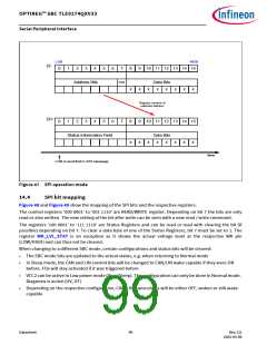
LSB
MSB
DI
0
1
2
3
4
5
6
7
8
x
9
x
10 11 12 13 14 15
R/W
Address Bits
Data Bits
x
x
x
x
x
x
Register content of
selected address
DO
0
1
2
3
4
5
6
7
8
x
9
x
10 11 12 13 14 15
Data Bits
Status Information Field
x
x
x
x
x
x
time
LSB is sent first in SPI message
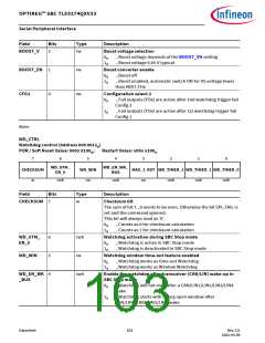
Figure 47 SPI operation mode
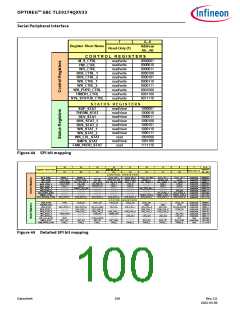
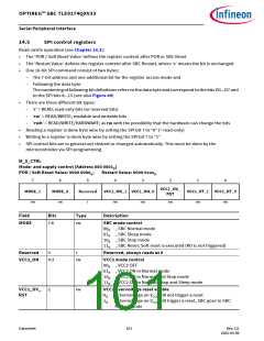
14.4
SPI bit mapping
Figure 48 and Figure 49 show the mapping of the SPI bits and the respective registers.
The control registers ‘000 0001’ to ‘001 1110’ are READ/WRITE register. Depending on bit 7 the bits are only
read or also written. The new setting of the bit after write can be seen with a new read / write command.
The registers ‘100 0001’ to ‘111 1110’ are Status Registers and can be read or read with clearing the bit (if
possible) depending on bit 7. To clear a data byte of one of the Status Registers, bit 7 must be set to 1. The
register WK_LVL_STAT is an exception as it shows the actual voltage level at the respective WK pin
(LOW/HIGH) and can thus not be cleared.
When changing to a different SBC mode, certain configurations and status bits will be cleared:
•
•
The SBC mode bits are updated to the actual status, e.g. when returning to Normal mode
In Sleep mode, the CAN and LIN control bits will be changed to CAN/LIN wake capable if they were ON
before. FOx will stay activated if it was triggered before
•
•
VCC2 can be active in Low power mode (Stop/Sleep). The configuration can only be done in Normal mode.
Diagnosis is active (UV, OT)
Depending on the respective configuration, CAN/LIN transceivers will be either OFF, woken or still wake
capable
Datasheet
99
Rev.2.0
2022-05-06

 INFINEON [ Infineon ]