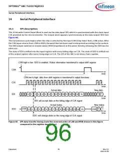
OPTIREG™ SBC TLE9274QXV33
Supervision functions
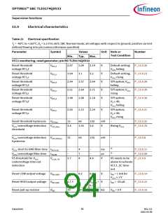
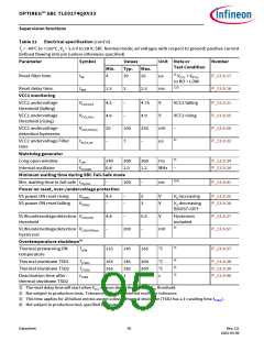
Table 21 Electrical specification (cont’d)
Tj = -40°C to +150°C; VS = 5.5 V to 28 V; SBC Normal mode; all voltages with respect to ground; positive current
defined flowing into pin (unless otherwise specified)
Parameter
Symbol
Values
Typ.
10
Unit Note or
Test Condition
Number
Min.
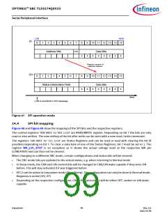
Max.
2)
Reset filter time
tRF
4
26
µs
V
< VRT1x
P_13.9.17
P_13.9.18
CC1
to RO = LOW
1)2)
Reset delay time
tRD1
1.5
2
2.5
ms
VCC2 monitoring
VCC2 undervoltage
threshold (falling)
VCC2,UV,f
VCC2,UV,r
VCC2,UV,hys
tVCC2,UV
4.5
4.6
20
–
–
4.75
4.9
250
–
V
VCC2 falling
VCC2 rising
P_13.9.21
P_13.9.55
P_13.9.56
P_13.9.22
VCC2 undervoltage
threshold (rising)
–
V
VCC2 undervoltage
detection hysteresis
100
7
mV
µs
–
2)
VCC2 undervoltage Filter
time
Watchdog generator
Long open window
Internal oscillator
4)
tLW
240
0.8
300
1.0
360
1.2
ms
P_13.9.34
P_13.9.24
fCLKSBC
MHz
–
Minimum waiting time during SBC Fail-Safe mode
2)3)
Min. waiting time in fail-safe tFS,min
–
100
–
ms
P_13.9.41
Power on reset, over-/undervoltage protection
VS power ON reset rising
VS power ON reset falling
VPOR,r
VPOR,f
4.5
–
–
–
5
3
V
V
VS increasing
P_13.9.25
P_13.9.26
VS decreasing
BOOST=OFF
VLINundervoltagedetection VLIN,UVD
threshold
4.8
–
–
5.5
–
V
Hysteresis
included
4)
P_13.9.27
P_13.9.57
VLINundervoltagedetection VLIN,UVD,hys
200
mV
hysteresis
Overtemperature shutdown4)
4)
Thermal prewarning ON
temperature
TjPW
125
145
165
°C
P_13.9.37
4)
4)
2)
Thermal shutdown TSD1
Thermal shutdown TSD2
TjTSD1
TjTSD2
tTSD2
165
165
–
185
185
1
200
200
–
°C
°C
s
P_13.9.38
P_13.9.39
P_13.9.40
Deactivation time after
thermal shutdown TSD2
1) The reset delay time will start when VCC1 crosses above the selected Vrtx threshold.
2) Not subject to production tests. Tolerance defined by internal oscillator tolerance.
3) This time applies for all failure entries except a device thermal shutdown (TSD2 has a 1 s waiting time tTSD2).
4) Not subject to production test, specified by design.
Datasheet
95
Rev.2.0
2022-05-06

 INFINEON [ Infineon ]