OPTIREG™ SBC TLE9274QXV33
Serial Peripheral Interface
14
Serial Peripheral Interface
14.1
SPI description
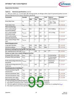
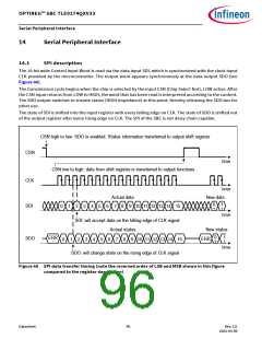
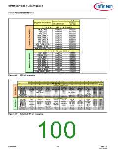
The 16-bit wide Control Input Word is read via the data input SDI, which is synchronized with the clock input
CLK provided by the microcontroller. The output word appears synchronously at the data output SDO (see
Figure 46).
The transmission cycle begins when the chip is selected by the input CSN (Chip Select Not), LOW active. After
the CSN input returns from LOW to HIGH, the word that has been read is interpreted according to the content.
The SDO output switches to tristate status (HIGH impedance) at this point, thereby releasing the SDO bus for
other use.
The state of SDI is shifted into the input register with every falling edge on CLK. The state of SDO is shifted out
of the output register after every rising edge on CLK. The SPI of the SBC is not daisy chain capable.
CSN high to low: SDO is enabled. Status information transferred to output shift register
CSN
time
CSN low to high: data from shift register is transferred to output functions
CLK
time
Actual data
New data
0 1
+ +
SDI
0 1 2 3 4 5 6 7 8 9 10 11 12 13 14 15
time
SDI: will accept data on the falling edge of CLK signal
Actual status
New status
0
1
+
ERR
SDO
ERR
0 1 2 3 4 5 6 7 8 9 10 11 12 13 14 15
-
+
time
SDO: will change state on the rising edge of CLK signal
Figure 46 SPI data transfer timing (note the reversed order of LSB and MSB shown in this figure
compared to the register description)
Datasheet
96
Rev.2.0
2022-05-06

 INFINEON [ Infineon ]