OPTIREG™ SBC TLE9274QXV33
Supervision functions
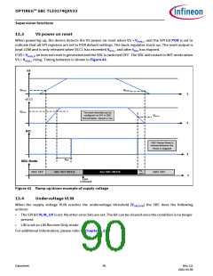
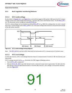
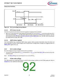
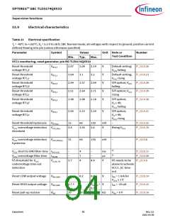
13.9
Electrical characteristics
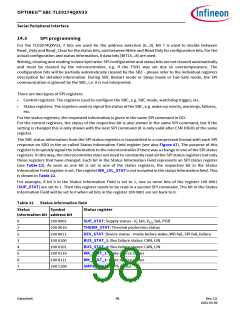
Table 21 Electrical specification
Tj = -40°C to +150°C; VS = 5.5 V to 28 V; SBC Normal mode; all voltages with respect to ground; positive current
defined flowing into pin (unless otherwise specified)
Parameter
Symbol
Values
Typ.
Unit Note or
Test Condition
Number
Min.
Max.
VCC1 monitoring, reset generator; pin RO TLE9274QXV33
Reset threshold
voltage RT1,f
VRT1,f
VRT1,r
VRT2,f
VRT2,r
VRT3,f
2.97
3.04
2.44
2.51
1.98
3.04
3.14
3.2
V
V
V
V
V
Default setting; P_13.9.20
V
CC1 falling
Default setting; P_13.9.23
CC1 rising
Reset threshold
voltage RT1,r
3.1
V
Reset threshold
voltage RT2,f
2.57
2.64
2.08
2.64
2.71
2.18
SPI option; VCC1 P_13.9.28
falling
Reset threshold
voltage RT2,r
SPI option; VCC1 P_13.9.29
rising
Reset threshold
voltage RT3,f
SPI option;
VS ≥ 4V;
P_13.9.30
P_13.9.31
V
CC1 falling
Reset threshold
voltage RT3,r
VRT3,r
2.05
2.15
2.24
V
SPI option;
VS ≥ 4V;
V
CC1 rising
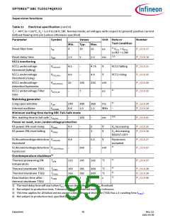
Reset threshold hysteresis VRT,hys
CC1 overvoltage detection VCC1,OV,r
15
66
130
3.6
mV
V
–
P_13.9.32
P_13.9.70
V
3.4
3.55
Rising VCC1
threshold
VCC1 overvoltage detection VCC1,OV,hys
15
66
130
mV
–
P_13.9.8
hysteresis
2)
2)
VCC1 short to GND filter time tVCC1,SC
–
4
7
4
–
ms
µs
V
P_13.9.11
P_13.9.58
P_13.9.9
V
CC1 overvoltage filter time tOV,filt
–
–
VS threshold for VCC1
undervoltage time out
detection
VS,UV_TO
3.7
4.4
VS needs to be
above to activate
VCC1_SC time-
out
Reset LOW output voltage
VRO,HIGH
–
0.2
–
0.4
V
IRO = 1 mA for
VCC1 ≥ 1 V
P_13.9.14
P_13.9.15
P_13.9.16
Reset HIGH output voltage VRO,LOW
0.7 ×
VCC1µC
VCC1µC + V
0.3 V
IRO = -20 µA
Reset pull-up resistor
RRO
10
20
40
kΩ
VRO = 0 V
Datasheet
94
Rev.2.0
2022-05-06

 INFINEON [ Infineon ]