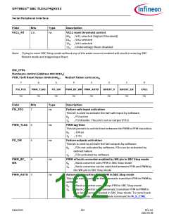
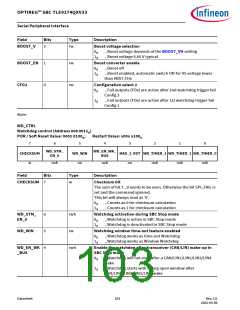
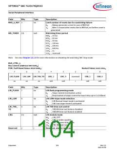
OPTIREG™ SBC TLE9274QXV33
Serial Peripheral Interface
14.5
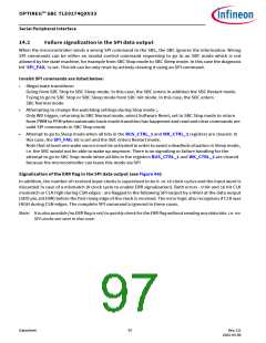
SPI control registers
Read-/write operation (see Chapter 14.3):
•
•
•
The ‘POR / Soft Reset Value’ defines the register content after POR or SBC Reset
The ‘Restart Value’ defines the register content after SBC Restart, where ‘x’ means the bit is unchanged
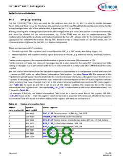
One 16-bit SPI command consist of two bytes:
–
–
The 7-bit address and one additional bit for the register access mode and
Following the data byte
The numbering of following bit definitions refers to the data byte and correspond to the bits D0...D7 and
to the SPI bits 8...15 (see also Figure 49)
•
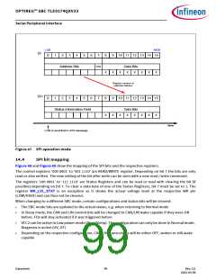
There are three different bit types:
–
–
–
‘r’ = READ; read-only bits (or reserved bits)
‘rw’ = READ/WRITE; readable and writable bits
‘rwh’ = READ/WRITE/HARDWARE; as rw with the possibility that the hardware can change the bits
•
•
•
Reading a register is done byte wise by setting the SPI bit 7 to “0” (= read-only)
Writing to a register is done byte wise by setting the SPI bit 7 to “1”
SPI control bits are in general not cleared or changed automatically. This must be done by the
microcontroller via SPI programming
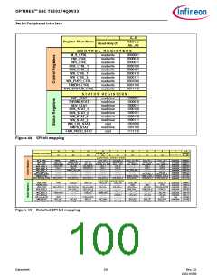
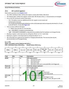
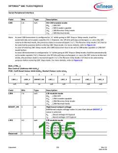
M_S_CTRL
Mode- and supply control (Address 000 0001B)
POR / Soft Reset Value: 0000 0000B;
Restart Value: 0000 0xxxB
7
6
5
4
3
2
1
0
VCC1_OV_
RST
MODE_1
MODE_0
Reserved
VCC2_ON_1 VCC2_ON_0
VCC1_RT_1 VCC1_RT_0
R
rw
rw
r
rw
rw
rw
rw
rw
Field
Bits
Type
Description
MODE
7:6
rw
SBC mode control
00B , SBC Normal mode
01B , SBC Sleep mode
10B , SBC Stop mode
11B , SBC Reset: Soft reset is executed (RO is not triggered)
Reserved
VCC2_ON
5
r
Reserved, always reads as 0
4:3
rw
VCC2 mode control
00B , VCC2 OFF
01B , VCC2 ON in Normal mode
10B , VCC2 ON in Normal and Stop mode
11B , VCC2 ON in Normal, Stop and Sleep mode
VCC1_OV_
RST
2
rw
VCC1 overvoltage reset enable
0B
1B
, Overvoltage on VCC1 will not trigger a reset
, Overvoltage on VCC1 will trigger a reset, SBC goes to SBC
Restart mode
Datasheet
101
Rev.2.0
2022-05-06

 INFINEON [ Infineon ]