OPTIREG™ SBC TLE9274QXV33
Serial Peripheral Interface
14.6
SPI status information registers
Read-/write operation (see Chapter 14.3):
•
One 16-bit SPI command consists of two bytes:
–
–
The 7-bit address and one additional bit for the register access mode and
Following the data byte will be ignored when accessing a status register
The numbering of following bit definitions refers to the data byte and correspond to the bits D0...D7 and
to the SPI bits 8...15 (see also Figure 49)
•
There are two different bit types:
–
–
‘r’ = READ: read-only bits (or reserved bits)
‘rc’ = READ/CLEAR: readable and clearable bits
•
•
•
Reading a register is done byte wise by setting the SPI bit 7 to “0” (= read-only)
Clearing a register is done byte wise by setting the SPI bit 7 to “1”
SPI status registers are in general not cleared or changed automatically (an exception are the WD_FAIL
bits). This must be done by the microcontroller via SPI command
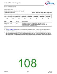
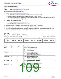
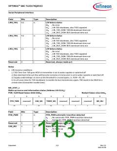
SUP_STAT
Supply voltage fail status (Address 100 0001B)
POR / Soft Reset Value: x000 0000B;
Restart Value: xxxx xx0xB
7
6
5
4
3
2
1
0
POR
VLIN_UV
VCC1_OV
VCC2_OT
VCC2_UV
VCC1_SC
reserved
VCC1_UV
r
rc
rc
rc
rc
rc
rc
r
rc
Field
Bits
Type
Description
POR
7
6
5
4
3
rc
rc
rc
rc
rc
Power-on-reset detection
0B
1B
, No POR
, POR occurred
VLIN_UV
VCC1_OV
VCC2_OT
VCC2_UV
VLIN undervoltage detection
0B
1B
, No VLIN undervoltage
, VLIN undervoltage detected
VCC1 overvoltage detection
0B
1B
, No VCC1 overvoltage
, VCC1 overvoltage detected
VCC2 overtemperature detection
0B
1B
, No overtemperature
, VCC2 overtemperature detected
VCC2 undervoltage detection
0B
1B
, No VCC2 undervoltage
, VCC2 undervoltage detected
Datasheet
109
Rev.2.0
2022-05-06

 INFINEON [ Infineon ]