AN985B/BX
Registers and Descriptors Description
ꢀꢁ ꢀꢂ ꢃꢄ ꢃꢅ ꢃꢆ ꢃꢇ ꢃꢈ ꢃꢉ ꢃꢀ ꢃꢃ ꢃꢁ ꢃꢂ ꢁꢄ ꢁꢅ ꢁꢆ ꢁꢇ ꢁꢈ ꢁꢉ ꢁꢀ ꢁꢃ ꢁꢁ ꢁꢂ ꢄ
ꢅ ꢆ ꢇ ꢈ ꢉ ꢀ ꢃ ꢁ ꢂ
5HV
UR
/7
&/6
UZ
UZ
Field
Res
LT
Bits
31:16
15:8
Type
ro
rw
Description
Reserved
Latency Timer
This value specifies the latency timer of the AN985B/BX in units of
CARDBUS bus clock. Once the AN985B/BX asserts FRAME#, the
latency timer starts to count. If the latency timer expires and the
AN985B/BX still asserted FRAME#, then the AN985B/BX will terminate
the data transaction as soon as its GNT# is removed.
CLS
7:0
rw
Cache Line Size
This value specifies the system cache line size in units of 32-bit double
words (DW). The AN985B/BX supports 8, 16, and 32 DW of cache line
size. This value is used by the AN985B/BX driver to program the cache
alignment bits (bit 14 and 15 of CSR0). The cache alignment bits are used
for cache oriented CARDBUS commands; say memory-read-line,
memory-read-multiple, and memory-write-and-invalidate.
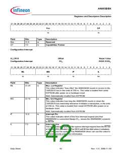
I/O Base Address
IOBA_CR4
I/O Base Address
Offset
10H
Reset Value
0000 0001H
ꢀꢁ ꢀꢂ ꢃꢄ ꢃꢅ ꢃꢆ ꢃꢇ ꢃꢈ ꢃꢉ ꢃꢀ ꢃꢃ ꢃꢁ ꢃꢂ ꢁꢄ ꢁꢅ ꢁꢆ ꢁꢇ ꢁꢈ ꢁꢉ ꢁꢀ ꢁꢃ ꢁꢁ ꢁꢂ ꢄ
ꢅ
ꢆ
ꢇ
ꢈ
ꢉ
5HV
UR
ꢀ
ꢃ
ꢁ
ꢂ
,2
6,
,2%$
UZ
UR
Field
Bits
Type
Description
IOBA
31:8
rw
I/O Base Address
This value indicate the base address of CARDBUS control and status
register (CSR0~28).
Res
IOSI
7:1
0
ro
ro
Reserved
I/O Space Indicator
1B
, means that the configuration registers map into the I/O space
Data Sheet
39
Rev. 1.51, 2005-11-30

 INFINEON [ Infineon ]