AN985B/BX
Registers and Descriptors Description
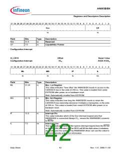
ꢀꢁ ꢀꢂ ꢃꢄ ꢃꢅ ꢃꢆ ꢃꢇ ꢃꢈ ꢃꢉ ꢃꢀ ꢃꢃ ꢃꢁ ꢃꢂ ꢁꢄ ꢁꢅ ꢁꢆ ꢁꢇ ꢁꢈ ꢁꢉ ꢁꢀ ꢁꢃ ꢁꢁ ꢁꢂ ꢄ
ꢅ
ꢆ
ꢇ
ꢈ
ꢉ ꢀ ꢃ ꢁ ꢂ
5HV
UR
&3
UR
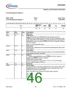
Field
Res
CP
Bits
31:8
7:0
Type
ro
ro
Description
Reserved
Capabilities Pointer
Configuration Interrupt
CI_CR15
Configuration Interrupt
Offset
3CH
Reset Value
XXXX 01XXH
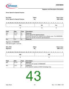
ꢀꢁ ꢀꢂ ꢃꢄ ꢃꢅ ꢃꢆ ꢃꢇ ꢃꢈ ꢃꢉ ꢃꢀ ꢃꢃ ꢃꢁ ꢃꢂ ꢁꢄ ꢁꢅ ꢁꢆ ꢁꢇ ꢁꢈ ꢁꢉ ꢁꢀ ꢁꢃ ꢁꢁ ꢁꢂ ꢄ
ꢅ
ꢆ
ꢇ
ꢈ
ꢉ ꢀ ꢃ ꢁ ꢂ
0/
0*
,3
,/
UZ
UR
UR
UR
Field
Bits
Type
Description
ML
31:24
ro
Max. Lat Register
This value indicates “how often” the AN985B/BX needs to access to the
CARDBUS bus in the units of 250 ns. This value is loaded from serial
EEPROM after power on or hardware reset.
Note:Automatically recalled from EEPROM.
MG
23:16
ro
Min. Gnt Register
This value indicates how long the AN985B/BX needs to retain the
CARDBUS bus ownership whenever it initiates a transaction, in the units
of 250 ns. This value is loaded from serial EEPROM after power on or
hardware reset.
Note:Automatically recalled from EEPROM.
IP
IL
15:8
7:0
ro
Interrupt Pin
This value indicates which of the four interrupt request pins that
AN985B/BX is connected.Always 01H: means the AN985B/BX connects
to INTA#
rw
Interrupt Line
This value indicates which of the system interrupt request lines the INTA#
of AN985B/BX is routed to. The BIOS will fill this field when it initializes
and configures the system. The AN985B/BX driver can use this value to
determine priority and vector information.
Data Sheet
42
Rev. 1.51, 2005-11-30

 INFINEON [ Infineon ]