2ED2110S06M
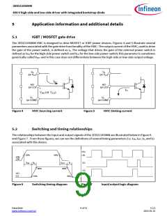
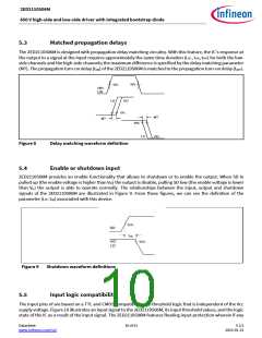
650 V high-side and low-side driver with integrated bootstrap diode
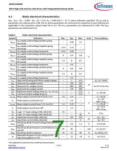
4.3
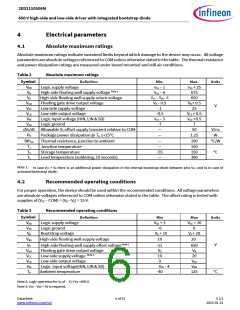
Static electrical characteristics
(VDD – VSS) = (VCC – COM) = (VB – VS) = 15 V, VSS = COM and TA = 25 °C unless otherwise specified. The VIN and IIN
parameters are referenced to COM. The VO and IO parameters are referenced to respective VS and COM and are
applicable to the respective output leads HO or LO. The VCCUV parameters are referenced to COM. The VBSUV
parameters are referenced to VS.
Table 4
Symbol
Static electrical characteristics
Definition
VDD supply undervoltage positive going
threshold
Min.
Typ.
Max.
Units
Test Conditions
VDDUV
—
2.85
3.1
+
VDD supply undervoltage negative going
threshold
VDD supply undervoltage hysteresis
VBS supply undervoltage positive going
threshold
VDDUV
2.55
0.05
8
2.75
0.09
8.9
—
—
-
VDDUVHY
VBSUV
9.8
+
V
VBS supply undervoltage negative going
threshold
VBS supply undervoltage hysteresis
VCC supply undervoltage positive going
threshold
VBSUV
7.3
—
8
8
8.7
—
-
VBSUVHY
0.9
8.9
VCCUV
9.8
+
VCC supply undervoltage negative going
threshold
VCCUV
7.3
8
8.7
-
VCCUVHY
ILK
IQBS
IQCC
VCC supply undervoltage hysteresis
High-side floating well offset supply leakage
Quiescent VBS supply current
Quiescent VCC supply current
Quiescent VDD supply current
—
—
—
—
—
—
—
1.6
0.9
1
150
600
110
—
—
12.5
230
900
200
0.15
0.15
—
VB = VS = 650 V
uA
V
VIN=0 V or VIN=VDD
IQDD
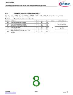
VOH High level output voltage drop, Vcc- VLO , VB- VHO
VOL Low level output voltage drop, VO
Io+mean Mean output current from 4.5 V to 7.5 V
IO = 20 mA
—
2.25
CL = 61 nF
VO = 0 V
PW ≤ 10 µs
CL = 61 nF
VO = 15 V
Io+
Io-mean Mean output current from 7.5 V to 4.5 V
Peak output current turn-on1
—
1.6
—
2.5
2.25
2.5
—
—
—
A
Io-
Peak output current turn-off1
PW ≤ 10 µs
VIH
VIL
IIN+
IIN-
Logic “1” input voltage (HIN, LIN & SD)
Logic “0” input voltage (HIN, LIN & SD)
70
—
—
—
—
—
215
—
—
30
270
5
%
µA
V
of VDD
Input bias current
VIN = VDD
VIN = 0 V
(HIN, LIN & SD)
Input bias current
(HIN, LIN & SD)
Bootstrap diode forward voltage between Vcc
and VB
Bootstrap diode forward current between Vcc
and VB
VFBSD
IFBSD
—
0.9
1.2
IF=0.3 mA
45
10
—
82
27
—
40
mA
Ω
VCC-VB=4 V
VF1=4V,VF2=5 V
Vcc=15 V
RBSD Bootstrap diode resistance
Allowable Negative VS pin voltage for IN
Signal propagation to HO
V
VS
-11
-10
1 Not subjected to production test, verified by characterization.
Datasheet
www.infineon.com/soi
7 of 31
V 2.5
2023-01-31

 INFINEON [ Infineon ]