2ED2110S06M
650 V high-side and low-side driver with integrated bootstrap diode
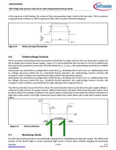
of the input pin is left floating, the output of the corresponding stage is held in the low state. This is achieved
using pull-down resistors on all the input pins (HIN, LIN) as shown in the block diagram.
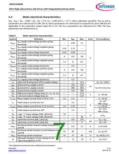
VIH
VIL
High
Low
Low
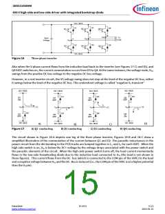
Figure 10
HIN & LIN input thresholds
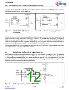
5.6
Undervoltage lockout
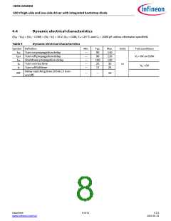
This IC provides undervoltage lockout protection on both the VCC (logic and low-side circuitry) power supply and
the VBS (high-side circuitry) power supply. Figure 11 is used to illustrate this concept; VCC (or VBS) is plotted over
time and as the waveform crosses the UVLO threshold (VCCUV+/- or VBSUV+/-) the undervoltage protection is enabled
or disabled.
Upon power-up, should the VCC voltage fail to reach the VCCUV+ threshold, the IC won’t turn-on. Additionally, if the
VCC voltage decreases below the VCCUV- threshold during operation, the undervoltage lockout circuitry will
recognize a fault condition and shutdown the high and low-side gate drive outputs.
Upon power-up, should the VBS voltage fail to reach the VBSUV+ threshold, the IC won’t turn-on. Additionally, if the
VBS voltage decreases below the VBSUV- threshold during operation, the undervoltage lockout circuitry will
recognize a fault condition, and shutdown the high-side gate drive outputs of the IC.
The UVLO protection ensures that the IC drives the external power devices only when the gate supply voltage is
sufficient to fully enhance the power devices. Without this feature, the gates of the external power switch could
be driven with a low voltage, resulting in the power switch conducting current while the channel impedance is
high; this could result in very high conduction losses within the power device and could lead to power device
failure.
VCC
(or VBS
)
VCCUV+
(or VBSUV+
)
VCCUV-
(or VBSUV-
)
Time
UVLO Protection
(Gate Drive Outputs Disabled)
Normal
Normal
Operation
Operation
Figure 11
UVLO protection
5.7
Bootstrap diode
An ultra-fast bootstrap diode is monolithically integrated for establishing the high side supply. The differential
resistor of the diode helps to avoid extremely high inrush currents when initially charging the bootstrap
Datasheet
www.infineon.com/soi
11 of 31
V 2.5
2023-01-31

 INFINEON [ Infineon ]