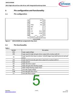
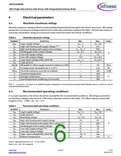
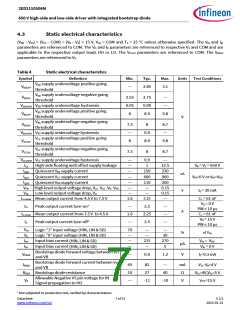
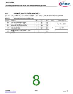
2ED2110S06M
650 V high-side and low-side driver with integrated bootstrap diode
5
Application information and additional details
5.1
IGBT / MOSFET gate drive
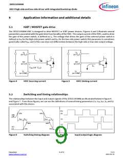
The 2ED2110S06M HVIC is designed to drive MOSFET or IGBT power devices. Figures 4 and 5 illustrate several
parameters associated with the gate drive functionality of the HVIC. The output current of the HVIC, used to drive
the gate of the power switch, is defined as IO. The voltage that drives the gate of the external power switch is
defined as VHO for the high-side power switch and VLO for the low-side power switch; this parameter is sometimes
generically called VOUT and in this case does not differentiate between the high-side or low-side output voltage.
VB
VB
(or VCC
)
(or VCC)
IO+
HO
HO
(or LO)
(or LO)
+
IO-
VHO (or VLO)
-
VS
VS
(or COM)
(or COM)
Figure 4
HVIC Sourcing current
Figure 5
HVIC Sinking current
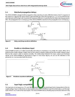
5.2
Switching and timing relationships
The relationships between the input and output signals of the 2ED2110S06M are illustrated below in Figure 6
and Figure 7. From these figures, we can see the definitions of several timing parameters (i.e. tON, tOFF, tR, and tF)
associated with this device.
50%
50%
HIN
LIN
tF
tON tR
tOFF
90%
90%
HO
LO
10%
10%
Figure 6
Switching timing diagram
Figure 7
Input/output logic diagram
Datasheet
www.infineon.com/soi
9 of 31
V 2.5
2023-01-31

 INFINEON [ Infineon ]