2ED2110S06M
650V high-side and low-side driver with integrated bootstrap diode
1
Table of contents
Features
Product summary ........................................................................................................................1
Product validation .......................................................................................................................................................1
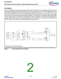
Description
2
1
2
Table of contents ................................................................................................................... 3
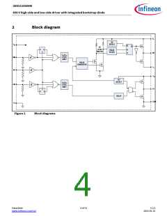
Block diagram........................................................................................................................ 4
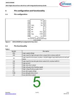
3
3.1
3.2
Pin configuration and functionality.......................................................................................... 5
Pin configuration.....................................................................................................................................5
Pin functionality ......................................................................................................................................5
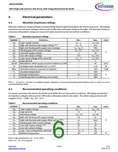
4
Electrical parameters ............................................................................................................. 6
Absolute maximum ratings.....................................................................................................................6
Recommended operating conditions.....................................................................................................6
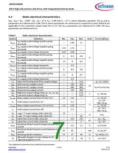
Static electrical characteristics...............................................................................................................7
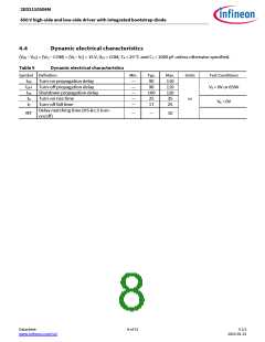
Dynamic electrical characteristics..........................................................................................................8
4.1
4.2
4.3
4.4
5
Application information and additional details.......................................................................... 9
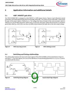
IGBT / MOSFET gate drive .......................................................................................................................9
Switching and timing relationships........................................................................................................9
Matched propagation delays ................................................................................................................10
Enable or shutdown input ....................................................................................................................10
Input logic compatibility.......................................................................................................................10
Undervoltage lockout ...........................................................................................................................11
Bootstrap diode.....................................................................................................................................11
Calculating the bootstrap capacitance CBS ..........................................................................................12
Tolerant to negative transients on input pins......................................................................................14
Negative voltage transient tolerance of VS pin....................................................................................14
NTSOA – Negative Transient Safe Operating Area ...............................................................................16
Higher headroom for input to output signal transmission with logic operation upto -11 V..............17
Maximum switching frequency.............................................................................................................17
PCB layout tips ......................................................................................................................................18
5.1
5.2
5.3
5.4
5.5
5.6
5.7
5.8
5.9
5.10
5.11
5.12
5.13
5.14
6
Parameters Trend Charts .......................................................................................................20
Qualification information.......................................................................................................26
Related products...................................................................................................................26
Package details.....................................................................................................................27
Part marking information ......................................................................................................28
7
8
9
10
11
11.1
Additional documentation and resources.................................................................................29
Infineon online forum resources ..........................................................................................................29
12
Revision history ....................................................................................................................30
Datasheet
www.infineon.com/soi
3 of 31
V 2.5
2023-01-31

 INFINEON [ Infineon ]