2ED2110S06M
650 V high-side and low-side driver with integrated bootstrap diode
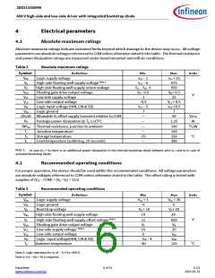
4
Electrical parameters
4.1
Absolute maximum ratings
Absolute maximum ratings indicate sustained limits beyond which damage to the device may occur. All voltage
parameters are absolute voltages referenced to COM unless otherwise stated in the table. The thermal resistance
and power dissipation ratings are measured under board mounted and still air conditions.
Table 2
Absolute maximum ratings
Symbol
VDD
VB
Definition
Logic supply voltage
Min.
VSS – 1
VCC – 6
VCC – VBS– 6
VS – 0.5
-1
Max.
VSS + 25
675
650
VB + 0.5
25
Units
High-side floating well supply voltage Note 1
High-side floating well supply return voltage
Floating gate drive output voltage
Low side supply voltage
VS
VHO
VCC
V
VLO
VIN
VSS
Low-side output voltage
Logic input voltage (HIN, LIN & SD)
Logic ground
–0.5
VSS – 5
-7
VCC + 0.5
VDD +0.5
7
dVS/dt Allowable VS offset supply transient relative to COM
—
—
50
1.25
V/ns
W
PD
Package power dissipation @ TA +25ºC
RthJA
TJ
TS
Thermal resistance, junction to ambient
Junction temperature
Storage temperature
—
—
-55
—
100
150
150
300
ºC/W
ºC
TL
Lead temperature (soldering, 10 seconds)
Note 1:
activated bootstrap diode.
In case VCC > VB there is an additional power dissipation in the internal bootstrap diode between pins VCC and VB in case of
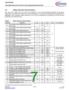
4.2
Recommended operating conditions
For proper operation, the device should be used within the recommended conditions. All voltage parameters
are absolute voltages referenced to COM unless otherwise stated in the table. The offset rating is tested with
supplies of (VCC – COM) = (VB – VS) = 15 V.
Table 3
Recommended operating conditions
Symbol
VDD
Definition
Logic supply voltage
Logic ground
Min
VSS + 3
-6
Max
VSS + 20
6
Units
VSS
VB
Bootstrap voltage
VS + 10
VS + 20
VBS
High-side floating well supply voltage
10
-11
VS
10
0
20
650
VB
V
VS
VHO
VCC
VLO
VIN
TA
High-side floating well supply offset voltage Note 2
Floating gate drive output voltage
Note 3
Low-side supply voltage
20
Low-side output voltage
Logic input voltage(HIN, LIN & SD)
Ambient temperature
VCC
VDD
125
VSS - 4
-40
ºC
Note 2: Logic operation for VS of – 11 V to +650 V.
Note 3: Vcc - Vss > 5V is required.
Datasheet
www.infineon.com/soi
6 of 31
V 2.5
2023-01-31

 INFINEON [ Infineon ]