2ED2110S06M
650V high-side and low-side driver with integrated bootstrap diode
Description
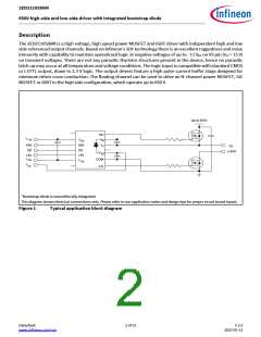
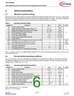
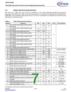
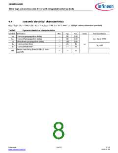
The 2ED2110S06M is a high voltage, high speed power MOSFET and IGBT driver with independent high and low
side referenced output channels. Based on Infineon’s SOI-technology there is an excellent ruggedness and noise
immunity with capability to maintain operational logic at negative voltages of up to - 11 VDC on VS pin (VCC = 15 V)
on transient voltages. There are not any parasitic thyristor structures present in the device, hence no parasitic
latch up may occur at all temperature and voltage conditions. The logic input is compatible with standard CMOS
or LSTTL output, down to 3.3 V logic. The output drivers feature a high pulse current buffer stage designed for
minimum driver cross-conduction. The floating channel can be used to drive an N-channel power MOSFET, SiC
MOSFET or IGBT in the high side configuration, which operate up to 650 V.
Up to 650V
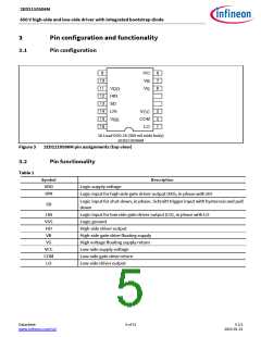
HO
V DD
VDD
HIN
SD
VB
VS
HIN
SD
TO
LOAD
VCC
COM
LO
LIN
LIN
V SS
VSS
VCC
*Bootstrap diode is monolithically integrated
This diagram shows electrical connections only. Please refer to our application notes and design tips for proper circuit board layout.
Figure 1
Typical application block diagram
Datasheet
www.infineon.com/soi
2 of 31
V 2.5
2023-01-31

 INFINEON [ Infineon ]