2ED2110S06M
650 V high-side and low-side driver with integrated bootstrap diode
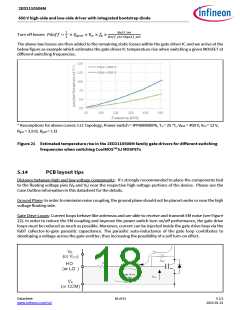
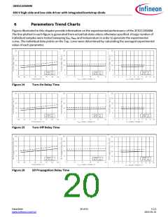
Figure 22
Avoid antenna loops
Supply Capacitor: It is recommended to place a bypass capacitor (CIN) between the VCC and COM pins. A ceramic
1μF ceramic capacitor is suitable for most applications. This component should be placed as close as possible
to the pins in order to reduce parasitic elements.
Routing and Placement: Power stage PCB parasitic elements can contribute to large negative voltage transients
at the switch node; it is recommended to limit the phase voltage negative transients. In order to avoid such
conditions, it is recommended to 1) minimize the high-side emitter to low-side collector distance, and 2)
minimize the low-side emitter to negative bus rail stray inductance. However, where negative VS spikes remain
excessive, further steps may be taken to reduce the spike. This includes placing a resistor (5 Ω or less) between
the VS pin and the switch node (see Figure 23 - A), and in some cases using a clamping diode between COM and
VS (see Figure 23- B). See DT04-4 at www.infineon.com for more detailed explanations.
Figure 23
Resistor between the VS pin and the switch node and clamping diode between COM and VS
Datasheet
www.infineon.com/soi
19 of 31
V 2.5
2023-01-31

 INFINEON [ Infineon ]