2ED2110S06M
650 V high-side and low-side driver with integrated bootstrap diode
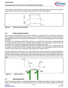
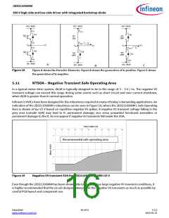
DC+ BUS
D3
D1
D5
D6
Q1
Q2
Q3
Q5
Q6
W
VS3
V
To
Load
Input
Voltage
VS2
U
VS1
D4
D2
Q4
DC- BUS
Figure 16
Three phase inverter
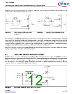
Also when the V phase current flows from the inductive load back to the inverter (see Figures 17 C) and D)), and
Q4 IGBT switches on, the current commutation occurs from D3 to Q4. At the same instance, the voltage node, VS2,
swings from the positive DC bus voltage to the negative DC bus voltage.
However, in a real inverter circuit, the VS voltage swing does not stop at the level of the negative DC bus, rather
it swings below the level of the negative DC bus. This undershoot voltage is called “negative VS transient”
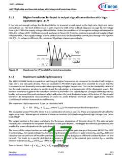
DC+ BUS
DC+ BUS
DC+ BUS
DC+ BUS
D3
D1
D2
D3
D4
Q1
ON
Q3
OFF
Q1
OFF
Q3
OFF
IU
IV
VS1
VS2
VS1
VS2
IV
IU
D2
Q2
OFF
Q4
ON
Q2
OFF
Q4
OFF
DC- BUS
DC- BUS
DC- BUS
DC- BUS
A)
D)
B)
C)
Figure 17
A) Q1 conducting
B) D2 conducting
C) D3 conducting
D) Q4 conducting
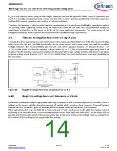
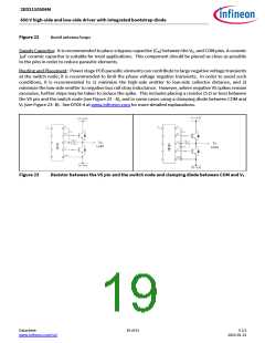
The circuit shown in Figure 18-A depicts one leg of the three phase inverter; Figures 18-B and 18-C show a
simplified illustration of the commutation of the current between Q1 and D2. The parasitic inductances in the
power circuit from the die bonding to the PCB tracks are lumped together in LC and LE for each IGBT. When the
high-side switch is on, VS1 is below the DC+ voltage by the voltage drops associated with the power switch and
the parasitic elements of the circuit. When the high-side power switch turns off, the load current momentarily
flows in the low-side freewheeling diode due to the inductive load connected to VS1 (the load is not shown in
these figures). This current flows from the DC- bus (which is connected to the COM pin of the HVIC) to the load
and a negative voltage between VS1 and the DC- Bus is induced (i.e., the COM pin of the HVIC is at a higher potential
than the VS pin).
Datasheet
www.infineon.com/soi
15 of 31
V 2.5
2023-01-31

 INFINEON [ Infineon ]