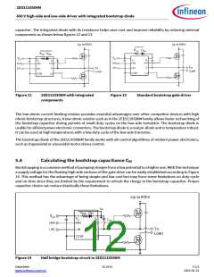
2ED2110S06M
650 V high-side and low-side driver with integrated bootstrap diode
DC+ BUS
LC1
DC+ BUS
DC+ BUS
+
VLC1
-
D1
D1
Q1
Q2
Q1
OFF
Q1
ON
+
LE1
LC2
IU
VLE1
-
VS1
VS1
VS1
-
IU
VLC2
+
D2
D2
-
Q2
OFF
Q2
OFF
VD2
+
-
LE2
DC- BUS
VLE2
+
DC- BUS
A
DC- BUS
C
B
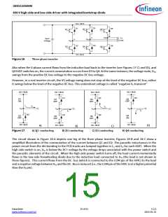
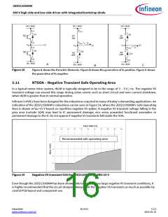
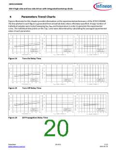
Figure 18
Figure A shows the Parasitic Elements. Figure B shows the generation of VS positive. Figure C shows
the generation of VS negative
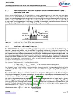
5.11
NTSOA – Negative Transient Safe Operating Area
In a typical motor drive system, dV/dt is typically designed to be in the range of 3 – 5 V / ns. The negative VS
transient voltage can exceed this range during some events such as short circuit and over-current shutdown,
when di/dt is greater than in normal operation.
Infineon’s HVICs have been designed for the robustness required in many of today’s demanding applications. An
indication of the 2ED2110S06M’s robustness can be seen in Figure 19, where the 2ED2110S06M’s Safe Operating
Area is shown at VBS=15 V based on repetitive negative VS spikes. A negative VS transient voltage falling in the
grey area (outside SOA) may lead to IC permanent damage; vice versa unwanted functional anomalies or
permanent damage to the IC do not appear if negative Vs transients fall inside the SOA.
Recommended safe operating area
Figure 19
Negative VS transient SOA for 2ED2110S06M @ VBS=15 V
Even though the 2ED2110S06M has been shown able to handle these large negative VS transient conditions, it
is highly recommended that the circuit designer always limit the negative VS transients as much as possible by
careful PCB layout and component use.
Datasheet
www.infineon.com/soi
16 of 31
V 2.5
2023-01-31

 INFINEON [ Infineon ]