2ED2110S06M
650 V high-side and low-side driver with integrated bootstrap diode
2
ꢋꢊꢎꢎ_푖ꢌꢉ
Turn off losses: ꢈ푑표푓푓 = × 푄푔ꢉꢊꢉ × 푉 × 푓 ×
푐푐
푝
2
ꢋꢊꢎꢎ_푖ꢌꢉꢍꢋ푔ꢊꢎꢎ_푒푥ꢉ
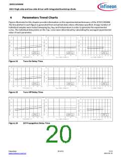
The above two losses are then added to the remaining static losses within the gate driver IC and we arrive at the
below figure as example which estimates the gate driver IC temperature rise when switching a given MOSFET at
different switching frequencies.
* Assumptions for above curves: LLC topology, Power switch = IPP60R600P6, Ta = 25 °C, VBUS = 400 V, VCC = 12 V,
Rgon = 3.9 Ω, Rgoff = 1 Ω
Figure 21 Estimated temperature rise in the 2ED2110S06M family gate drivers for different switching
frequencies when switching CoolMOSTM SJ MOSFETs
5.14
PCB layout tips
Distance between high and low voltage components: It’s strongly recommended to place the components tied
to the floating voltage pins (VB and VS) near the respective high voltage portions of the device. Please see the
Case Outline information in this datasheet for the details.
Ground Plane: In order to minimize noise coupling, the ground plane should not be placed under or near the high
voltage floating side.
Gate Drive Loops: Current loops behave like antennas and are able to receive and transmit EM noise (see Figure
22). In order to reduce the EM coupling and improve the power switch turn on/off performance, the gate drive
loops must be reduced as much as possible. Moreover, current can be injected inside the gate drive loop via the
IGBT collector-to-gate parasitic capacitance. The parasitic auto-inductance of the gate loop contributes to
developing a voltage across the gate-emitter, thus increasing the possibility of a self turn-on effect.
Datasheet
www.infineon.com/soi
18 of 31
V 2.5
2023-01-31

 INFINEON [ Infineon ]