2ED2110S06M
650 V high-side and low-side driver with integrated bootstrap diode
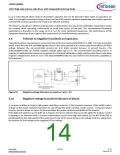
5.12
Higher headroom for input to output signal transmission with logic
operation upto -11 V
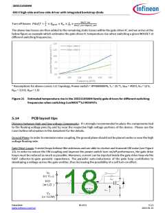
If there is not enough voltage for the level shifter to transmit a valid signal to the high side. High side driver
doesn’t turn on. The level shifter circuit is with respect to COM (refer to Block Diagram on page 4), the voltage
from VB to COM is the supply voltage of level shifter. Under the condition of VS is negative voltage with respect to
COM, the voltage of VS - COM is decreased, as shown in Figure 20. There is a minimum operational supply voltage
of level shifter, if the supply voltage of level shifter is too low, the level shifter cannot pass through HIN signal to
HO. If VB – VS voltage is different, the minimum VS voltage changes accordingly.
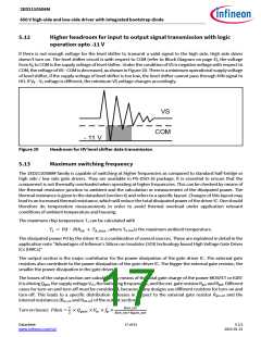
VS
COM
- 11 V
Figure 20
Headroom for HV level shifter data transmission
5.13
Maximum switching frequency
The 2ED2110S06M family is capable of switching at higher frequencies as compared to standard half-bridge or
high side / low side gate drivers. They are available in PG-DSO-16 package. It is essential to ensure that the
component is not thermally overloaded when operating at higher frequencies. This can be checked by means of
the thermal resistance junction to ambient and the calculation or measurement of the dissipated power. The
thermal resistance is given in the datasheet (section 4) and refers to a specific layout. Changes of this layout may
lead to an increased thermal resistance, which will reduce the total dissipated power of the driver IC. One should
therefore do temperature measurements in order to avoid thermal overload under application relevant
conditions of ambient temperature and housing.
The maximum chip temperature TJ can be calculated with
ꢆ = Pd ∙ 푅푡ℎ퐽ꢇ + ꢆ
, where TA_max is the maximum ambient temperature.
퐽
ꢇ_푚푎푥
The dissipated power Pd by the driver IC is a combination of several sources. These are explained in detail in the
application note “Advantages of Infineon’s Silicon on Insulator (SOI) technology based High Voltage Gate Driver
ICs (HVICs)”
The output section is the major contributor for the power dissipation of the gate driver IC. The external gate
resistors also contribute to the power dissipation of the gate driver IC. The bigger the external gate resistor, the
smaller the power dissipation in the gate driver.
The losses of the output section are calculated by means of the total gate charge of the power MOSFET or IGBT
it is driving Qgtot, the supply voltage VCC, the switching frequency fP, and the ext. gate resistor Rgon and Rgoff. Different
cases for turn-on and turn-off must be considered, because many designs use different resistors for turn-on and
turn-off. This leads to a specific distribution of losses in respect to the external gate resistor Rgxx_ext and the
internal resistances (Ron_int and Roff_int) of the output section.
2
ꢋꢊꢌ_푖ꢌꢉ
Turn on losses: ꢈ푑표푛 = × 푄푔ꢉꢊꢉ × 푉 × 푓 ×
푐푐
푝
2
ꢋꢊꢌ_푖ꢌꢉꢍꢋ푔ꢊꢌ_푒푥ꢉ
Datasheet
www.infineon.com/soi
17 of 31
V 2.5
2023-01-31

 INFINEON [ Infineon ]