2ED2110S06M
650 V high-side and low-side driver with integrated bootstrap diode
ILK_CAP is only relevant when using an electrolytic capacitor and can be ignored if other types of capacitors are
used. It is strongly recommend using at least one low ESR ceramic capacitor (paralleling electrolytic capacitor
and low ESR ceramic capacitor may result in an efficient solution).
The above CBS equation is valid for pulse by pulse considerations. It is easy to see, that higher capacitance values
are needed, when operating continuously at small duty cycles of low side. The recommended bootstrap
capacitance is therefore in the range up to 4.7 μF for most switching frequencies. The performance of the
integrated bootstrap diode supports the requirement for small bootstrap capacitances.
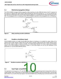
5.9
Tolerant to negative transients on input pins
Typically the driver's ground pin is connected close to the source pin of the MOSFET or IGBT. The microcontroller
which sends the HIN and LIN PWM signals refers to the same ground and in most cases there will be an offset
voltage between the microcontroller ground pin and driver ground because of ground bounce. The
2ED2110S06M family can handle negative voltage spikes up to 5 V. The recommended operating level is at
negative 4 V with absolute maximum of negative 5 V. Standard half bridge or high-side/low-side drivers only allow
negative voltage levels down to -0.3 V. The 2ED2110S06M family has much better noise immunity capability on
the input pins.
Figure 15
Negative voltage tolerance on inputs of up to –5 V
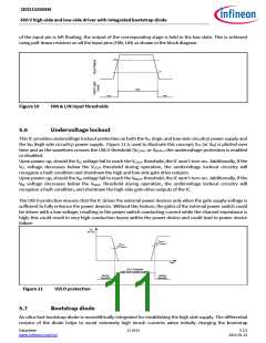
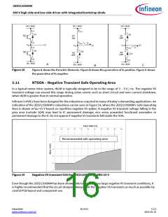
5.10
Negative voltage transient tolerance of VS pin
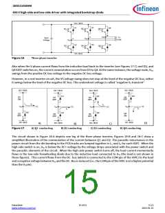
A common problem in today’s high-power switching converters is the transient response of the switch node’s
voltage as the power switches transition on and off quickly while carrying a large current. A typical 3-phase
inverter circuit is shown in Figure 16, here we define the power switches and diodes of the inverter.
If the high-side switch (e.g., the IGBT Q1 in Figures 16 and 17) switches from on to off, while the U phase current
is flowing to an inductive load, a current commutation occurs from high-side switch (Q1) to the diode (D2) in
parallel with the low-side switch of the same inverter leg. At the same instance, the voltage node VS1, swings from
the positive DC bus voltage to the negative DC bus voltage.
Datasheet
www.infineon.com/soi
14 of 31
V 2.5
2023-01-31

 INFINEON [ Infineon ]