2ED2110S06M
650 V high-side and low-side driver with integrated bootstrap diode
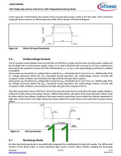
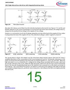
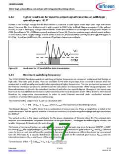
When the low side MOSFET turns on, it will force the potential of pin VS to GND. The existing difference between
the voltage of the bootstrap capacitor VCBS and VCC results in a charging current IBS into the capacitor CBS. The
current IBS is a pulse current and therefore the ESR of the capacitor CBS must be very small in order to avoid losses
in the capacitor that result in lower lifetime of the capacitor. This pin is on high potential again after low side is
turned off and high side is conducting current. But now the bootstrap diode DBS blocks a reverse current, so that
the charges on the capacitor cannot flow back to the capacitor CVCC. The bootstrap diode DBS also takes over the
blocking voltage between pin VB and VCC. The voltage of the bootstrap capacitor can now supply the high side
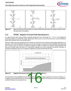
gate drive sections. It is a general design rule for the location of bootstrap capacitors CBS, that they must be placed
as close as possible to the IC. Otherwise, parasitic resistors and inductances may lead to voltage spikes, which
may trigger the undervoltage lockout threshold of the individual high side driver section. However, all parts of
the 2ED2110S06M family, which have the UVLO also contain a filter at each supply section in order to actively
avoid such undesired UVLO triggers.
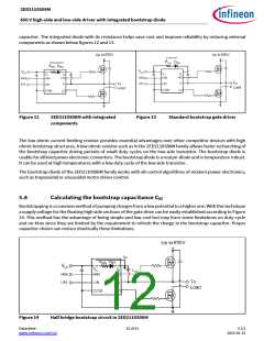
The current limiting resistor RBS according to Figure 14 reduces the peak of the pulse current during the low side
MOSFET turn-on. The pulse current will occur at each turn-on of the low side MOSFET, so that with increasing
switching frequency the capacitor CBS is charged more frequently. Therefore a smaller capacitor is suitable at
higher switching frequencies. The bootstrap capacitor is mainly discharged by two effects: The high side
quiescent current and the gate charge of the high side MOSFET to be turned on.
The minimum size of the bootstrap capacitor is given by
푄퐺푇푂푇
퐶퐵푆
=
∆푉퐵푆
VBS is the maximum allowable voltage drop at the bootstrap capacitor within a switching period, typically 1 V.
It is recommended to keep the voltage drop below the undervoltage lockout (UVLO) of the high side and limit
VBS ≤ (VCC – VF– VGSmin– VDSon
)
VGSmin > VBSUV- , VGSmin is the minimum gate source voltage we want to maintain and VBSUV- is the high-side supply
undervoltage negative threshold.
VCC is the IC voltage supply, VF is bootstrap diode forward voltage and VDSon is drain-source voltage of low side
MOSFET.
Please note, that the value QGTOT may vary to a maximum value based on different factors as explained below and
the capacitor shows voltage dependent derating behavior of its capacitance.
The influencing factors contributing VBS to decrease are:
- MOSFET turn on required Gate charge (QG)
- MOSFET gate-source leakage current (ILK_GS
)
- Floating section quiescent current (IQBS
- Floating section leakage current (ILK)
- Bootstrap diode leakage current (ILK_DIODE
- Charge required by the internal level shifters (푄퐿푆): typical 1nC
- Bootstrap capacitor leakage current (ILK_CAP
)
)
)
- High side on time (THON
)
Considering the above,
푄퐺푇푂푇 = 푄퐺 + 푄퐿푆 + (퐼ꢀ퐵푆 + 퐼퐿퐾 + 퐼퐿퐾 + 퐼퐿퐾
+ 퐼퐿퐾 ) ∗ ꢆ퐻푂푁
ꢅ퐴푃
ꢁꢂ
퐷ꢃꢄ퐷퐸
Datasheet
www.infineon.com/soi
13 of 31
V 2.5
2023-01-31

 INFINEON [ Infineon ]