IDT70825S/L
High-Speed 8K x 16 Sequential Access Random Access Memory
Industrial and Commercial Temperature Ranges
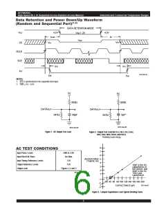
Data Retention and Power Down/Up Waveform
(Random and Sequential Port)(1,2)
DATA RETENTION MODE
4.5V
≥
VDR 2V
4.5V
VCC
tCDR
tR
VDR
VIH
CE
VIH
SCLK
SCE
tPD
tPU
ICC
3016 drw 04
I
SB
I
SB
NOTES:
1. SCE is synchronized to the sequential clock input.
2. CMD > VCC - 0.2V.
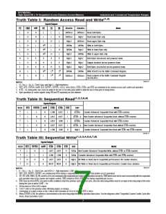
5V
5V
893Ω
893Ω
DATAOUT
DATAOUT
30pF
5pF*
347Ω
347Ω
,
3016 drw 06
3016 drw 05
Figure 1. AC Output Test Load
Figure 2. Output Test Load (for tCLZ, tBLZ, tOLZ, tCHZ,
tBHZ, tOHZ, tWHZ, tCKHZ, and tCKLZ)
*Including scope and jig.
8
7
6
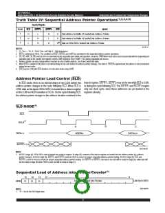
AC TEST CONDITIONS
Input Pulse Levels
GND to 3.0V
Input Rise/Fall Times
3ns Max.
1.5V
tAA/tCD/tEB
(Typical, ns)
5
4
3
2
1
Input Timing Reference Levels
Output Reference Levels
Output Load
1.5V
10pF is the I/O
capacitance of
this device, and
30pF is the AC
Test Load
Figures 1,2 and 3
3016 tbl 10
capacitance.
-1
-2
-3
20 40 60 80 100 120 140 160 180 200
,
3016 drw 07
CAPACITANCE (pF)
Figure 3. Lumped Capacitance Load Typical Derating Curve
6

 IDT [ INTEGRATED DEVICE TECHNOLOGY ]