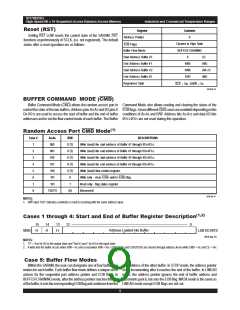
IDT70825S/L
High-Speed 8K x 16 Sequential Access Random Access Memory
Industrial and Commercial Temperature Ranges
Pin Descriptions: Random Access Port(1)
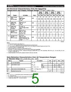
SYMBOL
NAME
I/O
DESCRIPTIONS
A
0-
A
12
Address Lines
Inputs/Outputs
Chip Enable
I
I
I
Address inputs to access the 8192-word (16-Bit) memory array.
Random access data inputs/outputs for 16-Bit wide data.
I/O
0-I/O15
CE
When CE is LOW, the random access port is enabled. When CE is HIGH, the random access port is disabled
into power-down mode and the I/O outputs are in the High-impedance state. All data is retained during CE =
VIH, unless it is altered by the sequential port. CE and CMD may not be LOW at the same time.
CMD
Control Register
Enable
I
I
When CMD is LOW, address lines A0-A2, R/W, and inputs/outputs I/O0-I/O12, are used to access the control
register, the flag register, and the start and end of buffer registers. CMD and CE may not be LOW at the same
time.
R/W
Read/Write Enable
Output Enable
If CE is LOW and CMD is HIGH, data is written into the array when R/W is LOW and read out of the array when
R/W is HIGH. If CE is HIGH and CMD is LOW, R/W is used to access the buffer command registers. CE and
CMD may not be LOW at the same time.
OE
I
I
When OE is LOW and R/W is HIGH, I/O
0-I/O15 outputs are enabled. When OE is HIGH, the I/O outputs are in
the High-impedance state.
Lower Byte, Upper
Byte Enables
When LB is LOW, I/O
0
-I/O
7
are accessible for read and write operations. When LB is HIGH I/O
0-I/O7 are tri-
LB, UB
stated and blocked during read and write operations. UB controls access for I/O
8
-I/O15 in the same manner and
is asynchronous from LB.
V
CC
Power Supply
Ground
I
I
Seven +5V power supply pins. All VCC pins must be connected to the same +5V VCC supply.
Ten ground pins. All ground pins must be connected to the same ground supply.
GND
3016 tbl 01
Pin Descriptions: Sequential Access Port(1)
SYMBOL
SI/O0-15
SCLK
NAME
I/O
DESCRIPTIONS
Sequential data inputs/outputs for 16-bit wide data.
SI/O
Inputs/Outputs
Clock
I
I
0
-SI/O15, SCE, SR/W, and SLD are registered on the LOW-to-HIGH transition of SCLK. Also, the sequential
access port address pointer increments by 1 on each LOW-to-HIGH transition of SCLK when CNTEN is LOW.
SCE
Chip Enable
I
When SCE is LOW, the sequential access port is enabled on the LOW-to-HIGH transition of SCLK. When SCE
is HIGH, the sequential access port is disabled into powered-down mode on the LOW-to-HIGH transition of
SCLK, and the SI/O outputs are in the High-impedance state. All data is retained, unless altered by the random
access port.
CNTEN
Control Enable
I
I
When CNTEN is LOW, the address pointer increments on the LOW-to-HIGH transition of SCLK. This function is
independent of CE.
SR/W
Read/Write Enable
When SR/W and SCE are LOW, a write cycle is initiated on the LOW-to-HIGH transition of SCLK. When SR/W is
HIGH, and SCE and SOE are LOW, a read cycle is initiated on the LOW-to-HIGH transition of SCLK. Termination
of a write cycle is done on the LOW-to-HIGH transition of SCLK if SR/W or SCE is HIGH.
SLD
Address Pointer
Load Control
I
When SLD is sampled LOW, there is an internal delay of one cycle before the address pointer changes. When
SLD is LOW, data on the inputs SI/O0-SI/O12 is loaded into a data-in registe r on the LOW-to-HIGH transition of
SCLK. On the cycle following SLD, the address pointer changes to the address location contained in the data-
in register. SSTRT and SSTRT may notbe LOW while SLD is LOW or during the cycle following SLD.
1
2
Load Start of
I
I
SSTRT
,
SSTRT1
2
Address Register
When SSTRT
1
or SSTRT2 is LOW, the startof address register #1 or #2 is loaded into the address pointer on
the LOW-to-HIGH transition of SCLK. The start address are stored in internal registers. SSTRT
may not be LOW while SLD is LOW or during the cycle following SLD.
1
and SSTRT
2
End of Buffer Flag
EOB
of the buffer registers. The flags can be cleared by either asserting RST LOW or by writing zero into Bit 0
and/or Bit 1 of the control register at address 101. EOB and EOB are dependent on separate internal
registers, and therefore separate match addresses.
1
or EOB2 is output LOW when the address pointer is incremented to match the address stored in the end
EOB
1,
EOB
2
1
2
SOE
RST
Output Enable
Reset
I
I
SOE controls the data outputs and is independentof SCLK. When SOE is LOW, output buffers and the
sequentially addressed data is output. When SOE is HIGH, the SI/O output bus is in the High-impedance state.
SOE is asynchronous to SCLK.
When RST is LOW, all internal registers are set to their default state, the address pointer is setto zero and the
EOB
1
and EOB2 flags are set HIGH. Rst is asynchronous to SCLK.
3016 tbl 02
NOTE:
1. "I/O" is bidirectional input and output. "I" is input and "O" is output.
6.42
3

 IDT [ INTEGRATED DEVICE TECHNOLOGY ]