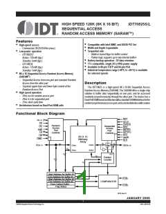
IDT70825S/L
High-Speed 8K x 16 Sequential Access Random Access Memory
Industrial and Commercial Temperature Ranges
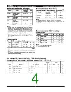
Absolute Maximum Ratings(1)
Recommended Operating
TemperatureandSupplyVoltage(1,2)
Symbol
Rating
Commercial
& Industrial
Unit
Grade
Ambient
Temperature
GND
Vcc
(2)
V
TERM
Te rminal Vo ltag e
with Respect
to GND
-0.5 to +7.0
V
Commercial
Industrial
0OC to +70OC
0V
0V
5.0V
5.0V
+
+
10%
10%
-40OC to +85OC
Temperature
Under Bias
-55 to +125
-65 to +150
50
oC
oC
T
BIAS
3016 tbl 04a
NOTES:
TSTG
Storage
Temperature
1. This is the parameter TA. This is the "instant on" case temperature.
2. Industrial temperature: for specific speeds, packages and powers contact your
sales office.
DC Output
Current
mA
IOUT
3016 tbl 03a
NOTES:
1. Stresses greater than those listed under ABSOLUTE MAXIMUM
RATINGS may cause permanent damage to the device. This is a stress
rating only and functional operation of the device at these or any other
conditions above those indicated in the operational sections of this
specification is not implied. Exposure to absolute maximum rating
conditions for extended periods may affect reliability.
2. VTERM must not exceed Vcc + 10% for more than 25% of the cycle time
or 10ns maximum, and is limited to < 20mA for the period of VTERM >
Vcc + 10%.
Recommended DC Operating
Conditions
Symbol
Parameter
Supply Voltage
GND Ground
Min.
Typ. Max. Unit
VCC
4.5
5.0
5.5
0
V
V
V
0
0
Capacitance
____
V
IH
Input High Voltage
Input Low Voltage
2.2
6.0(2)
0.8
(TA = +25°C, f = 1.0mhz, TQFP only)
____
VIL
-0.5(1)
V
Symbol
Parameter
Input Capacitance
Output Capacitance
Conditions(2)
IN = 3dV
OUT = 3dV
Max. Unit
3016 tbl 05
NOTES:
CIN
V
9
pF
1. VIL > –1.5V for pulse width less than 10ns.
2. VTERM must not exceed Vcc + 10%.
COUT
V
10
pF
3016 tbl 06
NOTES:
1. This parameter is determined by device characterization, but is not production
tested.
2. 3dV references the interpolated capacitance when the input and output signals
switch from 0V to 3V or from 3V to 0V.
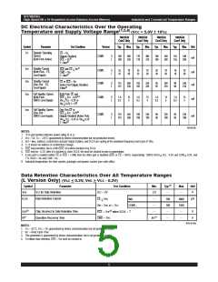
DC Electrical Characteristics Over the Operating
Temperature and Supply Voltage Range (VCC = 5.0V ± 10%)
70825S
70825L
Symbol
|ILI
|ILO
Parameter
Input Leakage Current
Test Conditions
CC = 5.5V, VIN = 0V to VCC
Min.
Max.
5
Min.
Max.
Unit
µA
µA
V
___
___
|
V
1
1
___
___
___
___
|
Output Leakage Current
Output Low Voltage
Output High Voltage
V
OUT = 0V to VCC
OL = +4mA
OH = -4mA
5
VOL
I
0.4
0.4
___
___
VOH
I
2.4
2.4
V
3016 tbl 07
4

 IDT [ INTEGRATED DEVICE TECHNOLOGY ]