IDT70825S/L
High-Speed 8K x 16 Sequential Access Random Access Memory
Industrial and Commercial Temperature Ranges
sequencingforthesequential(synchronous)accessport.
downfeature,controlledbyCE,permitstheon-chipcircuitryofeachport
FabricatedusingCMOShigh-performancetechnology,thismemory to enter a very low standby power mode.
device typically operates on less than 775mW of power at maximum
The IDT70825is packagedina 80-pinThinQuadFlatpack(TQFP)
high-speed clock-to-data and Random Access. An automatic power or 84-pin Pin Grid Array (PGA).
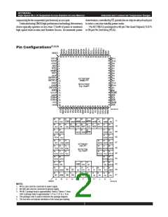
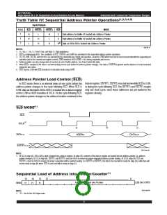
Pin Configurations(1,2,3)
INDEX
80 79 78 77 76 75 74 73 72 71 70 69 68 67 66 65 64 63 62 61
SI/O
1
A
A
A
A
A
A
A
A
A
A
V
V
A
A
11
10
9
60
59
1
SI/O
0
2
58
57
GND
N/C
SCE
SR/W
RST
SLD
3
4
5
6
7
8
8
56
55
7
6
54
53
52
51
5
4
SSTRT
2
3
9
IDT70825PF
PN80-1(4)
SSTRT
1
2
10
11
12
13
14
15
16
17
18
19
20
50
49
GND
GND
CNTEN
SOE
SCLK
GND
CC
CC
1
80-PinTQFP
Top View(5)
48
47
0
46
45
CMD
CE
LB
44
EOB
2
EOB
1
43 UB
42
VCC
R/W
OE
41
I/O0
21 22 23 24 25 26 27 28 29 30 31 32 33 34 35 36 37 38 39 40
,
3016 drw 02
63
61
V
60
58
55
54
51
48
46
45
42
11
GNDSSTRT2 SR/W
NC
GND NC
CNTEN
EOB
1
GND
I/O
1
CC
66
67
69
64
62
59
56
49
47
44
43
40
50
10
09
08
07
06
05
04
03
02
01
EOB
2
SOE RST
SCE
NC
SI/O
0
SI/O
1
SI/O3
I/O
2
SLD
I/O
0
65
57
53
41
39
52
SSTRT1
I/O
3
GND
SCLK GND
SI/O
2
VCC
68
38
37
I/O
4
V
CC
SI/O
4
SI/O5
72
75
76
71
73
33
35
34
I/O
7
I/O
6
SI/O8
SI/O
7
GND
GND
IDT70825G
G84-3(4)
70
74
32
31
36
I/O
9
I/O
5
I/O
8
SI/O9
SI/O10 SI/O
6
84-Pin PGA
Top View(5)
77
78
28
29
30
I/O10 I/O11
V
CC
SI/O12
V
CC SI/O11
79
80
26
27
I/O12
I/O13
83
SI/O14
23
SI/O13
25
81
7
11
12
CMD
I/O14
NC
V
CC
A2
NC SI/O15
82
1
2
5
8
10
14
17
20
22
24
OE
LB
A
7
A12
A
4
V
CC
A10
I/O15 GND
A
0
GND
84
3
4
6
9
15
13
16
18
19
21
NC
UB
CE
A8
R/W
A
1
A
5
A3
A
6
A
9
A11
A
B
C
D
E
F
G
H
J
K
L
INDEX
3016 drw 03
NOTES:
1. All VCC pins must be connected to power supply.
2. All GND pins must be connected to ground supply.
3. PN-80-1 package body is approximately 14mm x 14mm x 1.4mm.
G84-3 package body is approximately 1.21 in x 1.21 in x .16 in.
4. This package code is used to reference the package diagram.
5. This text does not indicate orientation of the actual part-marking.
2

 IDT [ INTEGRATED DEVICE TECHNOLOGY ]