IDT70825S/L
High-Speed 8K x 16 Sequential Access Random Access Memory
Industrial and Commercial Temperature Ranges
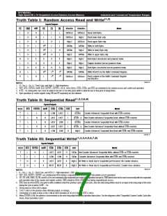
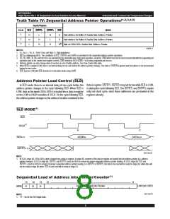
Truth Table IV: Sequential Address Pointer Operations(1,2,3,4,5)
Inputs/Outputs
SCLK
MODE
Start address for Buffer #1 loaded into Address Pointer.
Start address for Buffer #2 loaded into Address Pointer.
SLD
H
SSTRT
1
SSTRT
2
SOE
X
L
H
H
H
L
↑
↑
↑
H
X
(6)
L
H
H
Data on SI/O0-SI/O12 loaded into Address Pointer.
3016 tbl 14
NOTES:
1. H = VIH, L = VIL, X = Don't Care, and High-Z = High-impedance.
2. RST is continuously HIGH. The conditions of SCE, CNTEN, and SR/W are unrelated to the sequential address pointer operations.
3. CE, OE, R/W, LB, UB, and I/O0-I/O15 are unrelated to the sequential port control and operation, except for CMD which must not be used concurrently with the sequential port
operation (due to the counter and register control). CMD should be HIGH (CMD = VIH) during sequential port access.
4. Address pointer can also change when it reaches an end of buffer address. See Flow Control Bits table.
5. When SLD is sampled LOW, there is an internal delay of one cycle before the address pointer changes. The state of CNTEN is ignored and the address is not incremented
during the two cycles.
6. SOE may be LOW with SCE deselect or in the write mode using SR/W.
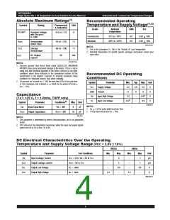
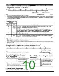
Address Pointer Load Control (SLD)
data-in register. SSTRT1, SSTRT2 may not be low while SLD is LOW,
or during the cycle following SLD. The SSTRT1 and SSTRT2 require
only one clock cycle, since these addresses are pre-loaded in the
registers already.
In SLD mode, there is an internal delay of one cycle before the
address pointer changes in the cycle following SLD. When SLD is
LOW, data on the inputs SI/O0-SI/O12 is loaded into a data-in register
on the LOW-to-HIGH transition of SCLK. On the cycle following SLD,
the address pointer changes to the address location contained in the
SLD MODE(1)
SLD
SCLK(1)
B
A
ADDRIN
C
SI/O0-12
DATAOUT
SSTRT(1 or 2)
3016 drw 08
NOTE:
1. At SCLK edge (A), SI/O0-SI/O12 data is loaded into a data-in register. At edge (B), contents of the data-in register are loaded into the address pointer (i.e. address
pointer changes). At SCLK edge (A), SSTRT1 and SSTRT2 must be HIGH to ensure for proper sequential address pointer loading. At SCLK edge (B), SLD and
SSTRT1,2 must be HIGH to ensure for proper sequential address pointer loading. For SSTRT1 or SSTRT2, the data to be read will be ready for edge (B), while data will
not be ready at edge (B) when SLD is used, but will be ready at edge (C).
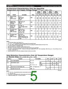
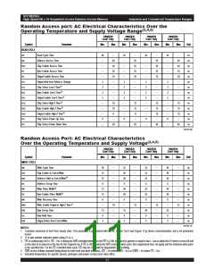
Sequential Load of Address into Pointer/Counter(1)
15
14
13
12 ------------------------------------------------------------------------------------------------------------ 0
Address Loaded into Pointer
LSB SI/O BITS
MSB
H
H
H
3016 drw 09
NOTE:
1. "H" = VIH for the SI/O intput state.
8

 IDT [ INTEGRATED DEVICE TECHNOLOGY ]