IDT70825S/L
High-Speed 8K x 16 Sequential Access Random Access Memory
Industrial and Commercial Temperature Ranges
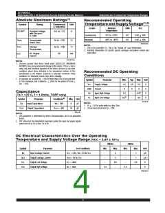
DC Electrical Characteristics Over the Operating
Temperature and Supply Voltage Range(1,2,8) (VCC = 5.0V ± 10%)
70825X20
70825X25
70825X35
70825X45
Com'l Only
Com'l Only
Com'l Only
Com'l Only
Symbol
Parameter
Test Condition
Version
Typ.
Max.
Typ.
Max.
Typ.
Max.
Typ.
Max.
Unit
ICC
Dynamic Operating
Current
(Both Ports Active)
CE = VIL
,
COM'L
S
L
180
180
380
330
170
170
360
310
160
160
340
290
155
155
340
290
Outputs Disabled
mA
(5)
SCE = VIL
(3)
f = fMAX
(7)
ISB1
Standby Current
(Both Ports - TTL
Level Inputs)
SCE and CE > VIH
CMD = VIH
COM'L
COM'L
S
L
25
25
70
50
25
25
70
50
20
20
70
50
16
16
70
50
mA
mA
(3)
f = fMAX
ISB2
Standby Current
(One Port - TTL
Level Inputs)
CE or SCE = VIH
S
L
115
115
260
230
105
105
250
220
95
95
240
210
90
90
240
210
Active Port Outputs Disabled,
(3)
f=fMAX
I
SB3
Full Standby Current
(Both Ports -
Both Ports CE and
(6,7)
SCE > VCC - 0.2V
COM'L
COM'L
S
L
1.0
0.2
15
5
1.0
0.2
15
5
1.0
0.2
15
5
1.0
0.2
15
5
mA
CMOS Level Inputs)
VIN > VCC - 0.2V or
V
IN < 0.2V, f = 0(4)
ISB4
Full Standby Current
(One Port -
CMOS Level Inputs)
One Port CE or
(6)
SCE > VCC - 0.2V
S
L
110
110
240
200
100
100
230
190
90
90
220
180
85
85
220
180
Outputs Disabled (Active Port)
mA
V
IN > VCC - 0.2V or VIN < 0.2V
(3)
f = fMAX
3016 tbl 08a
NOTES:
1. 'X' in part number indicates power rating (S or L).
2. VCC = 5V, TA = +25°C; guaranteed by device characterization but not production tested.
3. At f = fMAX, address, control lines (except Output Enable), and SCLK are cycling at the maximum frequency read cycle of 1/tRC.
4. f = 0 means no address or control lines change.
5. SCE may transition, but is LOW (SCE=VIL) when clocked in by SCLK.
6. SCE may be - 0.2V, after it is clocked in, since SCLK=VIH must be clocked in prior to powerdown.
7. If one port is enabled (either CE or SCE = LOW) then the other port is disabled (SCE or CE = HIGH, respectively). CMOS HIGH > Vcc - 0.2V and LOW < 0.2V, and
TTL HIGH = VIH and LOW = VIL.
8. Industrial temperature: for other speeds, packages and powers contact your sales office.
Data Retention Characteristics Over All Temperature Ranges
(L Version Only) (VLC < 0.2V, VHC > VCC - 0.2V)
Symbol
Parameter
Test Condition
Min.
Typ.(1)
Max.
Unit
V
___
___
V
DR
VCC for Data Retention
VCC = 2V
2.0
___
I
CCDR
Data Retention Current
µA
CE > VHC
IN = VHC or = VLC
IND.
COM'L.
100
4000
___
___
(2)
V
100
1500
(3)
CDR
SCE = VHC(4) when SCLK = ↑
CMD = VHC
___
___
t
Chip Deselect to Data Retention Time
Operation Recovery Time
V
(3)
___
___
tR
t
RC
V
3016 tbl 09a
NOTES :
1. TA = +25°C, VCC = 2V; guaranteed by device characterization but not production tested.
2. tRC = Read Cycle Time
3. This parameter is guaranteed by device characterization, but is not production tested.
4. To initiate data retention, SCE = VIH must be clocked in.
6.42
5

 IDT [ INTEGRATED DEVICE TECHNOLOGY ]