iC-MR 13-BIT S&H SIN/COS
INTERPOLATOR WITH CONTROLLER INTERFACES
Rev A1, Page 20/44
1.5
1.5
TUIN
Code
0
Addr 0x0E, bit 3
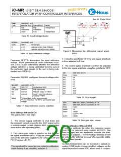
Nominal Rin() Internal Rui()
Mode
high
high
Voltage input
impedance
impedance
1
20 kΩ
5 kΩ
Voltage input
Px
Nx
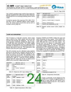
Table 15: Input voltage divider
VPNx
R0
VPx
DCPOS
Addr 0x0E, bit 6
VNx
Code
VREFI
2.5 V
Sensor type
GND
0
1
Lowside current drain (I Mode)
Highside current source (I Mode)
1.5 V
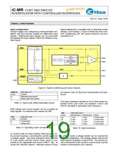
Figure 9: Measuring the differential signal ampli-
tudes
Table 16: Input reference voltage
3. Using fine gain factor GFS the sine signal amplitude
is then adjusted to 6 Vpp.
Parameter DCPOS determines the input reference
voltage. In the generation of center potentials SVDC
and CVDC it also determines whether the reference
voltage VREFin() is being subtracted from the sum of
the particular input signals or the sum is being sub-
tracted from VREFin().
4. The cosine signal amplitude can then be adjusted
to the sine signal amplitude using fine gain factor GFC.
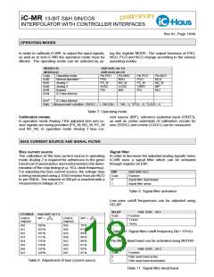
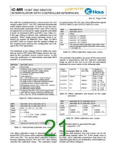
GR
Addr 0x02, bit 2:0
Code
0x0
0x1
0x2
0x3
0x4
0x5
0x6
0x7
Factor
2.0
Parameter SELREF configures the input voltage refer-
ence.
4.1
5.3
6.7
SELREF
Code
Addr 0x0D, bit 7:6
8.7
VREFin()
internal
internal
external
Pin function VREF
10.5
13.2
16.0
0x0, 0x1
0x2
high impedance
Output*: output of VREFI
0x3
Input**: external reference
replaces VREFI
Table 18: Coarse gain
Notes
*) Do not load, buffer recommended.
**) See Elec.Char. No.105 for permissible input
voltage.
GFS
GFC
Code
0x000
0x001
...
Addr 0x03, bit 6:0, Addr 0x02, bit 7:4
Addr 0x05, bit 2:0, Addr 0x04, bit 7:0
Table 17: Input reference source selection
Factor
1.0
1.0009
6.25(GFx/1984)
6.6245
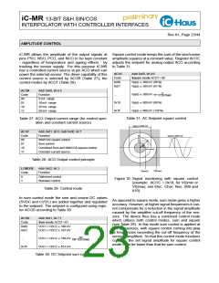
Gain settings SIN and COS
The gain is set in four steps:
0x7FF
Table 19: Fine gain sine, cosine
1. The sensor supply controller is shut down and
the constant current source for the ACO output set to
a suitable output current (register ADJ; current value
close to the later operating point).
Offset calibration SIN and COS
In order to calibrate the offset the reference source
must first be selected using register REFVOS. Two
fixed voltages and two dependent sources are avail-
able for this purpose. The fixed voltage sources should
be selected for external sensors which provide stable,
self-regulated signals.
2. The coarse gain range is selected so that differen-
tial signal amplitudes of ca. 6 Vpp are produced at the
core of the converter (signal PS_W versus NS_W and
PC_W versus NC_W).
So that photosensors can be operated in optical en-
coders iC-MR tracks changes in offset voltages via the
signal-dependent source VDC when used in conjunc-
The signals at the converter core output in calibration
mode Analog 1 are amplified by factor 3.

 ICHAUS [ IC-HAUS GMBH ]