iC-MR 13-BIT S&H SIN/COS
INTERPOLATOR WITH CONTROLLER INTERFACES
Rev A1, Page 18/44
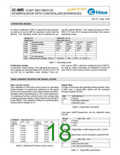
OPERATING MODES
In order to calibrate iC-MR, to adjust the input signals, ing the register MODE. The output functions of PSO,
as well as to test iC-MR the operation mode must be NSO, PCO and NCO change according to the various
altered. The operating mode can be selected by us- operating modes.
MODE(1:0)
MODE(4:2)
ADR 0x0F; bit 1:0
ADR 0x10; bit 2:0
Code
0x00
0x01
0x02
0x03
0x04
...
Operating mode
Normal operation *
Analog 1
Analog 2
Bypass
Pin PSO
PSO
PS_W
SVDC
PSI
Pin NSO
NSO
NS_W
CVDC
NSI
Pin PCO
PCO
PC_W
VREFI
PCI
Pin NCO
NCO
NC_W
IBP
NCI
iC-Haus internal
0x1F
iC-Haus internal
Note: *) Measurement condition: ENOCC = 1, ENOCM = 1, TIIN = 0, TIPOL = 0, TLDOS = 0
Table 7: Operating mode
Calibration modes
rent source (IBP), reference potential input (VREFI),
In operation mode Analog 1 the adjusted sine and co- as well as center potentials of calibration circuits for
sine signals are being provided (PS_W, NS_W, PC_W sine (SVDC) and cosine (CVDC) can be measured.
und NC_W). In operation mode Analog 2 bias cur-
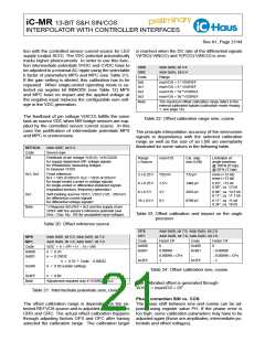
BIAS CURRENT SOURCE AND SIGNAL FILTER
Bias current source
Signal filter
The calibration of the bias current source in operating In order to decrease the adjusted analog signals’ noise
mode Analog 2 is required for adherence to the given iC-MR uses a signal filter which can be activated
Electrical Characteristics and instrumental in the deter- through register bit ENF.
mination of the chip timing (e.g. SCL clock frequency).
For adjusting the bias current source, the voltage drop
is being measured using a 10 kΩ resistor from pin NCO
to pin GNDA. The setpoint of 200 µA is reached with a
measurement voltage of 2 V.
ENF
Code
0
Addr 0x0F, bit 2
Function
Signal filter deactivated
Signal filter active
1
Table 9: Signal filter activation
Low pass cutoff frequencies can be adjusted using
SELBP.
SELBP
Addr. 0x0F; bit 3
Function
CFGBIAS Addr 0x0F, bit 7:4
Code
31
31
31−k
Code k
IBP ∼
Code k
(signed)
IBP ∼
31−k
0
1
7.5 kHz
15 kHz
(signed)
0x0
0x1
0x2
0x3
0x4
0x5
0x6
0x7
100 %
103 %
107 %
111 %
115 %
119 %
124 %
129 %
0x8
0x9
0xA
0xB
0xC
0xD
0xE
0xF
79 %
81 %
84 %
86 %
88 %
91 %
94 %
97 %
Table 10: Signal filter cutoff frequency (fin < 10 Hz)
The filter’s dead band can be activated using NEFDR.
NEFDR
Addr. 0x0C; bit 3
Function
Code
0
1
Filter dead band active
Table 8: Adjustment of bias current source
Filter dead band deactivated
Table 11: Signal filter dead band

 ICHAUS [ IC-HAUS GMBH ]