iC-MR 13-BIT S&H SIN/COS
INTERPOLATOR WITH CONTROLLER INTERFACES
Rev A1, Page 24/44
ACOC
Code
0x00
Addr 0x00, bit 4:0
Constant current source ACOT = 11
The control’s operating range and the input signal am-
plitudes supplied to the control unit are both monitored.
Should any error occur during monitoring, these can be
output.
I(ACO) ≈ 3.125 % Isc(ACO)
I(ACO) ≈ 6.250 % Isc(ACO)
0x01
...
I(ACO) ≈ 3.125 % * (Code + 1) * Isc(ACO)
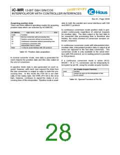
So that the signals at the input pins PSO, NSO, PCO,
and NCO can be calibrated without control interfer-
ence, the current source at pin ACO can be set to a
constant current (Table 28).
0x1F
Note
I(ACO) ≈ 100 % Isc(ACO)
Isc(ACO) see characteristics no. 802
Table 32: Setpoint current source (ACO output cur-
rent)
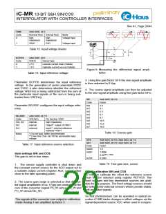
12-BIT A/D CONVERTER
The IC features a 12-bit A/D converter, which output Registers TEMPHI and TEMPLO define the upper and
data is stored in the TEMP register and can be read lower thresholds for error output. If the current con-
out from here through the interfaces. The A/D con- verter value is above TEMPHI or below TEMPLO, the
verter operates constantly, updating the data in regis- ERR_TMP alarm bit is set in the error register. The
ter TEMP after each conversion. The TEMP register internal ADC can be utilized to continuously record
cannot be read by bytewise access to addresses 0x6A an external temperature, for which a temperature-
and 0x6B, as otherwise it is not guaranteed that a con- dependent voltage is applied at pin ADC. This can be
tiguous data word is read out. The temperature data generated by a KTY temperature sensor. A tempera-
must be read out by the cyclic telegram.
ture monitor can be created using thresholds TEMPHI
and TEMPLO. By way of example, the following de-
The A/D converter can be calibrated using registers scribes the evaluation of temperature sensor KTY 84.
ADCSLOP and ADCOFF. Register ADCSLOP has 8
bits and is used to set the maximum voltage the con-
verter can process at pin ADC. The allocation of the
register data in ADCSLOP to the maximum voltage is
expressed in Table 33. Using the second calibration
register ADCOFF, which has 16 bits, an offset can be
added to the converter’s digital output data.
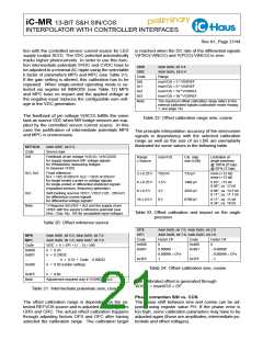
TEMPLO
TEMPHI
Code
Addr. 0x14...0x15;
R/W
Addr. 0x16...0x17;
R/W
Temperature threshold
0x7FFF
...
+3276.7 °C
...
0x07D0
...
+200.0 °C
...
ADCSLOP
Code
0x00
Addr. 0x11; bit 7...0
Full scale level for VDDA = 5V
2.0 V
R/W
0x0001
0x0000
0xFFFF
...
+0.1 °C
0.0 °C
-0.1 °C
0x01
2.00196 V
...
...
2.0 V + 1.96 mV * ADCSLOP
2.5 V
0xFE70
...
-40 °C
0xFF
...
0x8000
Note
-3276.8 °C
Table 33: Maximum ADC input voltage ADC
Thresholds for example KTY 84
Table 35: Temperature thresholds
ADCOFF
Addr. 0x12...0x13;
Function
R/W
Code
0x7FFF
...
TEMP = TEMP(int) + 32767
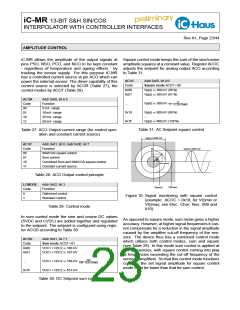
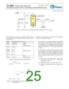
Figure 11 shows a schematic circuit diagram for the
evaluation of the KTY. A resistor of approximately 2.3
kΩ is switched in series with the KTY sensor to lin-
earize the voltage supplied by the KTY. This results in
a linear temperature voltage.
0x0001
0x0000
0xFFFF
...
TEMP = TEMP(int) + 1
TEMP = TEMP(int)
TEMP = TEMP(int) - 1
0x8000
TEMP = TEMP(int) - 32768
Table 34: Digital temperature offset value

 ICHAUS [ IC-HAUS GMBH ]